
EP2S15F672C3N
| Part Description |
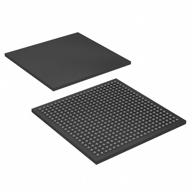
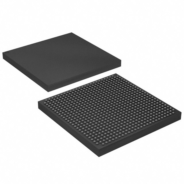
Stratix® II Field Programmable Gate Array (FPGA) IC 366 419328 15600 672-BBGA |
|---|---|
| Quantity | 939 Available (as of June 14, 2026) |

| Product Category | Field Programmable Gate Array (FPGA) |
|---|---|
| Manufacturer | Intel |
| Manufacturing Status | Obsolete |
| Manufacturer Standard Lead Time | Contact Us |
| Datasheet |
Specifications & Environmental
| Device Package | 672-FBGA (27x27) | Grade | Commercial | Operating Temperature | 0°C – 85°C | ||
|---|---|---|---|---|---|---|---|
| Package / Case | 672-BBGA | Number of I/O | 366 | Voltage | 1.15 V - 1.25 V | ||
| Mounting Method | Surface Mount | RoHS Compliance | RoHS Compliant | REACH Compliance | REACH Unaffected | ||
| Moisture Sensitivity Level | 3 (168 Hours) | Number of LABs/CLBs | 780 | Number of Logic Elements/Cells | 15600 | ||
| Number of Gates | N/A | ECCN | 3A991D | HTS Code | 8542.39.0001 | ||
| Qualification | N/A | Total RAM Bits | 419328 |
Overview of EP2S15F672C3N – Stratix® II FPGA, 15,600 logic elements, 366 I/O, 672‑BBGA
The EP2S15F672C3N is a Stratix® II field programmable gate array (FPGA) IC from Intel designed for commercial-temperature applications. It integrates 15,600 logic elements, approximately 0.42 Mbits of embedded RAM, and 366 I/O pins in a 672‑BBGA package to support complex digital logic, high‑density interfacing, and on‑chip memory requirements.
Built on the Stratix II device architecture, the device includes on‑chip clock management (PLLs), DSP circuitry, TriMatrix memory structures and advanced I/O capabilities documented in the Stratix II handbook, making it suitable for designs that require dense logic resources and flexible I/O and clocking.
Key Features
- Core Logic 15,600 logic elements and 780 logic array blocks (LABs) provide a high degree of programmable logic integration for custom digital designs.
- Embedded Memory Approximately 0.42 Mbits (419,328 bits) of on‑chip RAM for buffering, FIFOs, and local data storage.
- I/O Density 366 I/O pins support complex interfacing requirements and high pin‑count system connections.
- Clocking & DSP Stratix II architecture includes PLLs and digital signal processing blocks as described in the device handbook for flexible clock management and arithmetic processing.
- Advanced I/O & Termination Documentation covers advanced I/O standards, high‑speed differential I/O with DPA support, programmable drive strength and on‑chip termination options.
- Configuration & Test Device handbook details JTAG boundary‑scan support, SignalTap II embedded logic analysis, and multiple configuration schemes for development and production testing.
- Package & Mounting 672‑BBGA package (supplier package: 672‑FBGA, 27 × 27 mm) in a surface‑mount form factor for board‑level integration.
- Power & Temperature Core supply range 1.15 V to 1.25 V. Commercial operating temperature range 0 °C to 85 °C.
- Compliance RoHS compliant.
Typical Applications
- High‑performance digital signal processing — Use on‑chip DSP blocks and the device's RAM for filtering, transforms, and other compute‑intensive DSP tasks.
- External memory interfaces and buffering — TriMatrix memory and configurable I/O enable interfacing to external memory and high‑throughput data buffering.
- Custom logic prototyping and system control — Dense logic resources and comprehensive configuration/test features support prototype and production control logic implementations.
- High‑density I/O bridging — 366 I/O pins and advanced I/O standard support enable protocol bridging, parallel interfaces, and multi‑lane signal routing.
Unique Advantages
- Highly integrated logic and memory: 15,600 logic elements combined with approximately 0.42 Mbits of embedded RAM reduce external component count for many designs.
- Extensive I/O resources: 366 I/O pins accommodate complex system connectivity without immediate need for external I/O expanders.
- Comprehensive clocking and DSP support: Stratix II architecture provides PLLs and DSP blocks for flexible clock management and arithmetic acceleration.
- Production and debug tooling: Built‑in support for JTAG and SignalTap II documented in the handbook simplifies in‑system debug and production testing.
- Commercial temperature rating: Specified for 0 °C to 85 °C operation to match standard commercial application environments.
- RoHS compliant packaging: 672‑BBGA surface‑mount package meets RoHS requirements for lead‑free assembly processes.
Why Choose EP2S15F672C3N?
The EP2S15F672C3N offers a balanced combination of logic density, embedded memory, and high I/O capacity within the Stratix II architecture. It is positioned for commercial designs that require integrated DSP capability, flexible clocking, and robust on‑chip memory and interfacing documented in the Stratix II device handbook.
This device is suited to customers developing high‑density FPGA implementations where on‑chip resources and comprehensive configuration/test support reduce system complexity. Leveraging Intel's Stratix II documentation and features provides a clear design path for scaling and integration into production designs.
Request a quote or submit a product inquiry to obtain pricing, lead times, and availability for the EP2S15F672C3N.


Date Founded: 1968
Headquarters: Santa Clara, California, USA
Employees: 130,000+
Revenue: $54.23 Billion
Certifications and Memberships: ISO9001:2015, ISO14001:2015, ISO17025:2017, ISO27001:2022, ISO45001:2018, ISO50001:2018


