
EP2S15F672C5
| Part Description |
Stratix® II Field Programmable Gate Array (FPGA) IC 366 419328 15600 672-BBGA |
|---|---|
| Quantity | 132 Available (as of June 15, 2026) |

| Product Category | Field Programmable Gate Array (FPGA) |
|---|---|
| Manufacturer | Intel |
| Manufacturing Status | Obsolete |
| Manufacturer Standard Lead Time | Contact Us |
| Datasheet |
Specifications & Environmental
| Device Package | 672-FBGA (27x27) | Grade | Commercial | Operating Temperature | 0°C – 85°C | ||
|---|---|---|---|---|---|---|---|
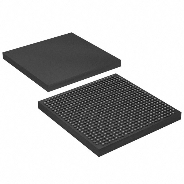
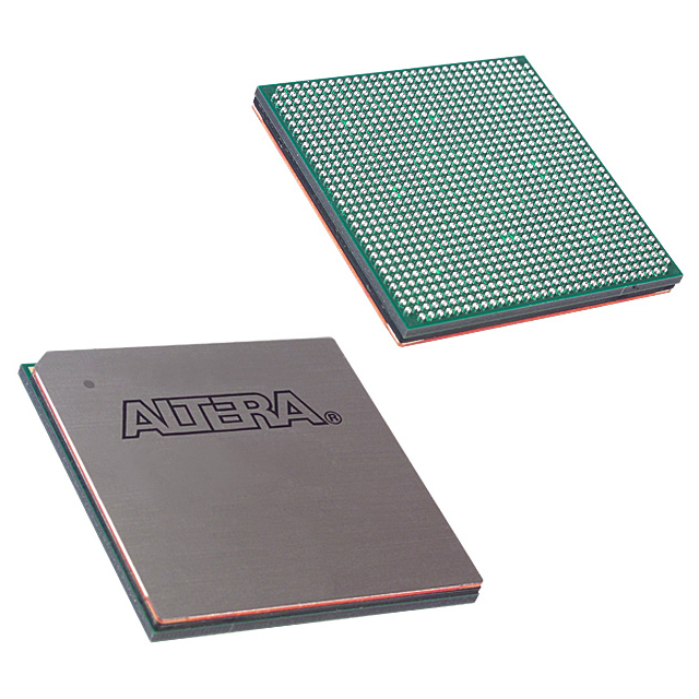
| Package / Case | 672-BBGA | Number of I/O | 366 | Voltage | 1.15 V - 1.25 V | ||
| Mounting Method | Surface Mount | RoHS Compliance | RoHS non-compliant | REACH Compliance | REACH Unaffected | ||
| Moisture Sensitivity Level | 3 (168 Hours) | Number of LABs/CLBs | 780 | Number of Logic Elements/Cells | 15600 | ||
| Number of Gates | N/A | ECCN | 3A991D | HTS Code | 8542.39.0001 | ||
| Qualification | N/A | Total RAM Bits | 419328 |
Overview of EP2S15F672C5 – Stratix® II Field Programmable Gate Array (FPGA) IC 366 419328 15600 672-BBGA
The EP2S15F672C5 is an Intel Stratix II family FPGA optimized for designs that require substantial logic capacity, on-chip memory, and a high I/O count in a compact surface-mount package. This device integrates 15,600 logic elements across 780 logic array blocks and approximately 419,328 bits of embedded RAM, making it suitable for complex digital signal processing, protocol bridging, and custom logic implementations.
Stratix II series architecture provides advanced on-chip resources—including dedicated DSP blocks, programmable clocking with PLLs, and a flexible I/O structure—while this specific device is offered in a 672-BBGA (supplier package: 672-FBGA, 27×27) with a supply voltage range of 1.15 V to 1.25 V and a commercial operating temperature range of 0 °C to 85 °C. The device is RoHS compliant and intended for surface-mount assembly.
Key Features
- Core Logic 15,600 logic elements implemented across 780 logic array blocks (LABs) to support medium-to-high density custom digital designs.
- Embedded Memory Approximately 0.42 Mbits (419,328 bits) of on-chip RAM to support buffering, lookup tables, and local storage for datapath and control logic.
- I/O Capacity 366 user I/O pins for flexible interfacing to external devices, memory, and peripherals.
- Clocking & Configuration Stratix II family features in-device PLLs and multi-tier clock networks to support complex timing architectures and clock domain management.
- DSP & High-performance Blocks Series-level Stratix II architecture includes dedicated digital signal processing blocks to accelerate arithmetic and signal-processing functions.
- Package & Mounting 672-BBGA surface-mount package (supplier package: 672-FBGA, 27×27) for compact board-level integration.
- Power & Supply Core supply voltage range of 1.15 V to 1.25 V to match system power rails in targeted designs.
- Commercial Temperature & Compliance Rated for 0 °C to 85 °C operation and RoHS compliant for regulatory adherence in commercial products.
- Configuration & Test Support Series documentation details JTAG boundary-scan support and embedded logic analysis capabilities for development and validation.
Typical Applications
- Signal Processing Implement DSP functions and accelerated arithmetic pipelines using the device’s dedicated DSP resources and on-chip RAM.
- Memory Interface Controllers Build external RAM controllers and interface logic using abundant I/O and Stratix II external RAM interfacing features.
- Protocol Bridging & Interface Gateways Translate or bridge between different digital interfaces with the device’s high I/O count and flexible I/O structure.
- Custom Logic & Accelerator Modules Deploy application-specific accelerators and control logic leveraging 15,600 logic elements and programmable clocking.
Unique Advantages
- High logic density: 15,600 logic elements enable implementation of sizable custom datapaths and control logic without external ASICs.
- Substantial on-chip RAM: Approximately 0.42 Mbits of embedded memory reduces external memory dependency for many buffering and LUT needs.
- Extensive I/O: 366 I/O pins support multi-channel interfacing and complex board-level connectivity.
- Advanced clocking and DSP support: Stratix II architecture includes PLLs and DSP blocks to simplify high-performance signal and timing designs.
- Compact, production-ready package: 672-BBGA (672-FBGA, 27×27) surface-mount package suited for dense PCB layouts.
- Commercial-grade and RoHS compliant: Rated for 0 °C to 85 °C operation and compliant with RoHS directives for commercial products.
Why Choose EP2S15F672C5?
The EP2S15F672C5 delivers a balanced combination of logic capacity, embedded memory, and extensive I/O in a Stratix II FPGA platform. It is well suited for engineers designing mid-to-high complexity digital systems that require on-chip DSP resources, versatile clocking, and dense I/O in a compact BGA footprint.
Backed by the Stratix II device family documentation from Intel/Altera, this device is appropriate for teams needing a documented architecture with integrated configuration and test features for development and production deployments.
Request a quote or submit an inquiry to purchase EP2S15F672C5. Provide your required quantity and delivery timeframe to receive a tailored response from our sales channel.


Date Founded: 1968
Headquarters: Santa Clara, California, USA
Employees: 130,000+
Revenue: $54.23 Billion
Certifications and Memberships: ISO9001:2015, ISO14001:2015, ISO17025:2017, ISO27001:2022, ISO45001:2018, ISO50001:2018


