
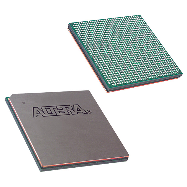
EP2S180F1020C4
| Part Description |
Stratix® II Field Programmable Gate Array (FPGA) IC 742 9383040 179400 1020-BBGA |
|---|---|
| Quantity | 1,528 Available (as of June 18, 2026) |

| Product Category | Field Programmable Gate Array (FPGA) |
|---|---|
| Manufacturer | Intel |
| Manufacturing Status | Obsolete |
| Manufacturer Standard Lead Time | Contact Us |
| Datasheet |
Specifications & Environmental
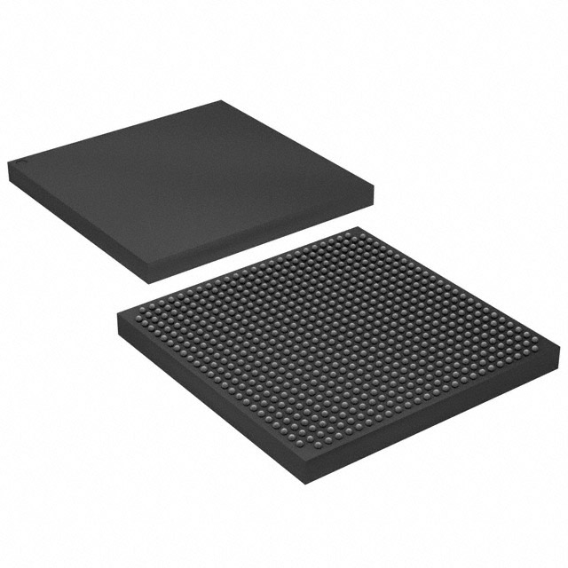
| Device Package | 1020-FBGA (33x33) | Grade | Commercial | Operating Temperature | 0°C – 85°C | ||
|---|---|---|---|---|---|---|---|
| Package / Case | 1020-BBGA | Number of I/O | 742 | Voltage | 1.15 V - 1.25 V | ||
| Mounting Method | Surface Mount | RoHS Compliance | RoHS non-compliant | REACH Compliance | REACH Unaffected | ||
| Moisture Sensitivity Level | 4 (72 Hours) | Number of LABs/CLBs | 8970 | Number of Logic Elements/Cells | 179400 | ||
| Number of Gates | N/A | ECCN | 3A001A7A | HTS Code | 8542.39.0001 | ||
| Qualification | N/A | Total RAM Bits | 9383040 |
Overview of EP2S180F1020C4 – Stratix® II Field Programmable Gate Array (FPGA) IC 742 9383040 179400 1020-BBGA
The EP2S180F1020C4 is a Stratix® II family FPGA from Intel, supplied in a 1020-BBGA (1020-FBGA, 33×33) surface-mount package for commercial-grade designs. It combines a large logic fabric with substantial on-chip memory and a high pin count to address complex digital processing, interface, and system-integration requirements.
With 179,400 logic elements and approximately 9.38 Mbits of embedded memory, this device targets high-density logic implementation, heavy buffering, and designs that require extensive I/O connectivity within a 0 °C to 85 °C operating range and a 1.15 V–1.25 V core supply window.
Key Features
- Logic Capacity — 179,400 logic elements to implement large-scale combinational and sequential logic, and to accommodate complex state machines and glue logic.
- On‑Chip Memory — Approximately 9.38 Mbits of embedded RAM for buffering, FIFOs, and local data storage without external memory for many use cases.
- I/O Density — 742 I/O pins to support extensive external interfaces, parallel buses, and multi-channel connectivity.
- High‑Performance Architecture — Stratix II architecture elements described in the device handbook such as adaptive logic modules, dedicated DSP circuitry, and TriMatrix memory structure for flexible routing and performance-oriented designs.
- DSP & Clocking — On‑chip digital signal processing blocks and enhanced/fast PLL and clock network features referenced in the device handbook for clock management and signal processing tasks.
- Advanced I/O Capabilities — Support for high‑speed differential I/O, MultiVolt I/O interface options, programmable drive strength, on‑chip termination, and advanced I/O standard support as documented in the device handbook.
- Configuration & Debug — JTAG boundary-scan support, SignalTap II embedded logic analyzer, and multiple configuration schemes referenced in the device handbook to simplify bring-up and in-system debug.
- Package & Power — 1020-BBGA surface-mount package (supplier device package: 1020-FBGA, 33×33) and a specified core voltage supply range of 1.15 V to 1.25 V for proper power planning.
- Commercial Grade & Compliance — Commercial grade device with an operating range of 0 °C to 85 °C and RoHS-compliant manufacturing.
Typical Applications
- High‑Performance Signal Processing — Uses on‑chip DSP blocks and large logic capacity to implement filtering, FFTs, and real‑time data processing pipelines.
- High‑Speed Communications — Leverages abundant I/O and high‑speed differential I/O support to implement multi‑lane interfaces and protocol bridging.
- Memory Interface & Controller Design — Combines many I/Os and substantial embedded RAM for external memory interfacing, buffering, and controller logic.
- System Integration & Prototyping — Large logic element count and configurable I/O make the device suitable for integrating multiple subsystems or validating complex designs in hardware.
Unique Advantages
- Large Logic Resource: 179,400 logic elements provide the density required to implement complex SoC glue logic and multi‑function designs without partitioning across devices.
- Significant Embedded Memory: Approximately 9.38 Mbits of on‑chip RAM reduces external memory dependency for many buffering and local storage needs.
- Extensive I/O: 742 I/Os enable broad connectivity options for multi‑channel interfaces, parallel buses, and mixed‑signal front ends.
- Comprehensive Architecture: Stratix II architectural features (DSP blocks, PLLs, TriMatrix memory, advanced I/O) deliver flexible implementation choices documented in the device handbook.
- Deployment‑Ready Package: 1020‑BBGA (33×33) surface‑mount package supports dense PCB integration while meeting commercial operating temperature requirements.
- Regulatory Compliance: RoHS‑compliant manufacturing helps meet environmental requirements for commercial electronics products.
Why Choose EP2S180F1020C4?
The EP2S180F1020C4 delivers a high-density Stratix II FPGA option for commercial designs that require a combination of abundant logic elements, sizable on‑chip memory, and very high I/O counts. Its documented architecture—covering adaptive logic modules, DSP blocks, advanced clocking, and robust I/O features—supports implementation of demanding processing, interface, and integration tasks.
This device is well suited for engineering teams building high‑complexity digital systems, communication interfaces, and signal processing solutions who need a commercially graded FPGA with detailed architectural and configuration support available in the device handbook.
Request a quote or submit an RFQ today to check pricing and availability for EP2S180F1020C4.


Date Founded: 1968
Headquarters: Santa Clara, California, USA
Employees: 130,000+
Revenue: $54.23 Billion
Certifications and Memberships: ISO9001:2015, ISO14001:2015, ISO17025:2017, ISO27001:2022, ISO45001:2018, ISO50001:2018


