
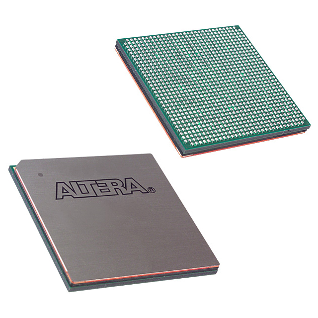
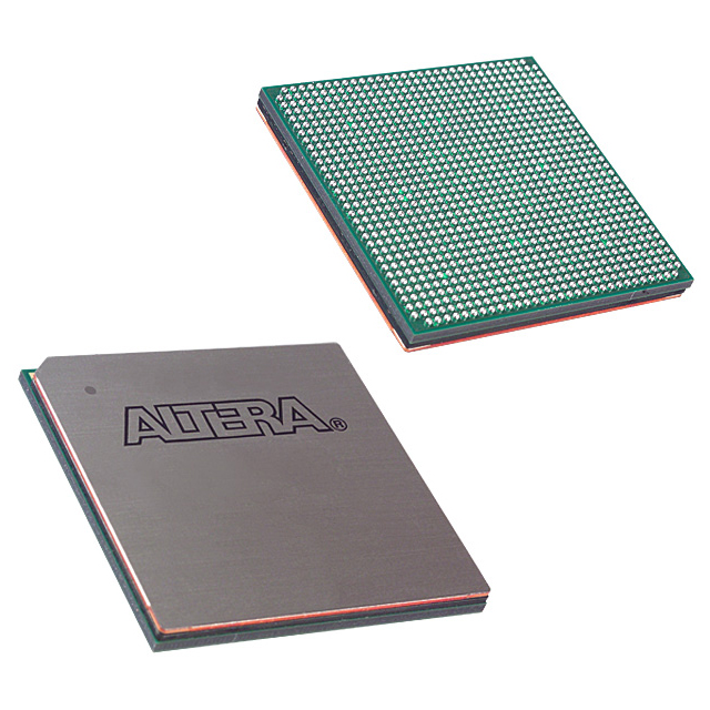
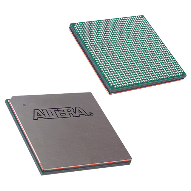
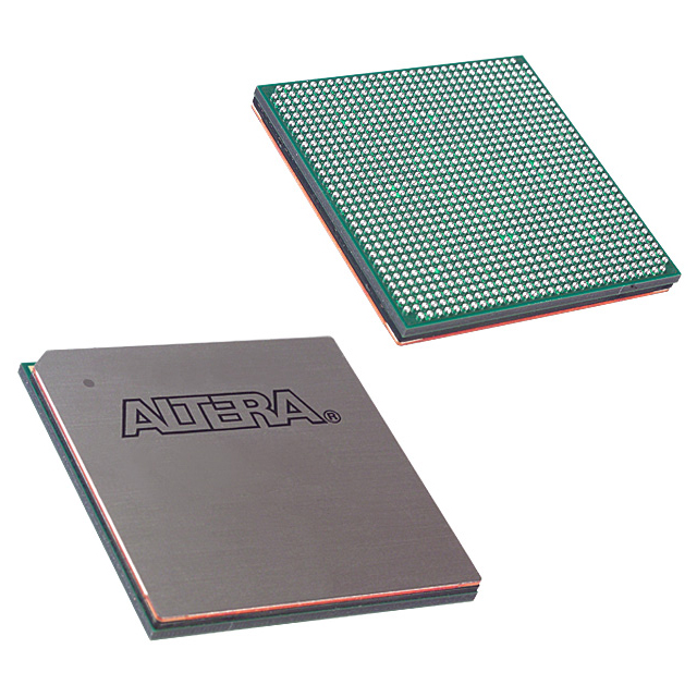
EP2S180F1020C4N
| Part Description |
Stratix® II Field Programmable Gate Array (FPGA) IC 742 9383040 179400 1020-BBGA |
|---|---|
| Quantity | 502 Available (as of October 8, 2026) |
| Product Category | Field Programmable Gate Array (FPGA) |
|---|---|
| Manufacturer | Intel |
| Manufacturing Status | Obsolete |
| Manufacturer Standard Lead Time | Contact Us |
| Datasheet |
Specifications & Environmental
| Device Package | 1020-FBGA (33x33) | Grade | Commercial | Operating Temperature | 0°C – 85°C | ||
|---|---|---|---|---|---|---|---|
| Package / Case | 1020-BBGA | Number of I/O | 742 | Voltage | 1.15 V - 1.25 V | ||
| Mounting Method | Surface Mount | RoHS Compliance | RoHS Compliant | REACH Compliance | REACH Unaffected | ||
| Moisture Sensitivity Level | 3 (168 Hours) | Number of LABs/CLBs | 8970 | Number of Logic Elements/Cells | 179400 | ||
| Number of Gates | N/A | ECCN | 3A001A7A | HTS Code | 8542.39.0001 | ||
| Qualification | N/A | Total RAM Bits | 9383040 |
Overview of EP2S180F1020C4N – Stratix® II Field Programmable Gate Array (FPGA) IC, 179,400 logic elements, 742 I/O, 1020-BBGA
The EP2S180F1020C4N is a Stratix II family FPGA from Intel (Altera) designed for high-density, programmable logic implementations. The device combines a large logic fabric with embedded memory and configurable I/O to address demanding digital designs.
With 179,400 logic elements, approximately 9.38 Mbits of embedded memory, and 742 I/O pins in a 1020-BBGA package, this Stratix II device targets applications that require extensive on-chip resources, flexible clocking and advanced I/O capabilities while operating within a commercial temperature range.
Key Features
- Logic Capacity Provides 179,400 logic elements for complex combinational and sequential logic integration.
- Embedded Memory Approximately 9.38 Mbits of on-chip RAM to support buffers, FIFOs and local data storage.
- High Pin Count I/O 742 I/O pins enable dense external interfacing and support for multi-channel systems.
- Advanced I/O Architecture Stratix II I/O features described in the device handbook include Double Data Rate I/O, multivoltage I/O support, programmable drive strength, on-chip termination and high-speed differential I/O options.
- Clocking and Timing Integrated PLLs and hierarchical/global clock networks provide flexible clock management for synchronous designs.
- DSP and Signal Processing Blocks The device family documentation lists dedicated Digital Signal Processing blocks for arithmetic-intensive logic and high-throughput data paths.
- Memory Architecture TriMatrix memory architecture and multiple memory block sizes enable adaptable on-chip memory partitioning and efficient memory interfacing.
- Configuration & Test Support Includes IEEE 1149.1 JTAG boundary-scan support and embedded logic analysis capabilities (SignalTap II) described in the Stratix II handbook.
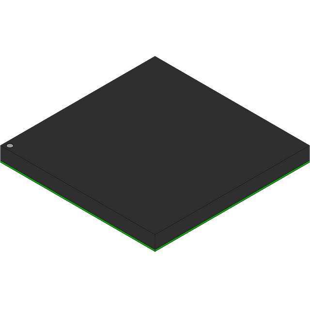
- Package & Supply Supplied in a 1020-BBGA (supplier package: 1020-FBGA, 33×33) with a core voltage range of 1.15 V to 1.25 V.
- Commercial Temperature Grade Rated for operation from 0 °C to 85 °C and RoHS compliant.
Typical Applications
- High-performance signal processing: Use the embedded DSP blocks and large on-chip RAM to implement filters, FFTs and custom data-path accelerators.
- Network and communications equipment: Leverage the high logic density and 742 I/O pins for packet processing, protocol offload, and multiport interfaces.
- Test and measurement systems: Deploy flexible I/O standards, on-chip timing resources and SignalTap II support to instrument and validate complex digital designs.
- Embedded compute and control: Consolidate multiple functions into a single device using the abundant logic elements and memory to reduce BOM and interconnect complexity.
Unique Advantages
- High integration density: 179,400 logic elements enable implementation of large logic designs without partitioning across multiple devices.
- Substantial on-chip memory: Approximately 9.38 Mbits of embedded RAM supports data buffering and local storage, reducing dependence on external memory.
- Extensive external interfacing: 742 I/O pins accommodate wide buses, multiple high-speed links, and diverse peripheral connectivity.
- Flexible clocking and DSP support: Built-in PLLs, hierarchical clock networks and DSP blocks simplify design of high-throughput, timing-sensitive systems.
- Robust configuration and test features: JTAG boundary-scan and embedded logic analysis capabilities help streamline development, debug and production testing.
- Commercial-grade deployment: Rated for 0 °C to 85 °C operation and RoHS compliant, suitable for a wide range of commercial applications.
Why Choose EP2S180F1020C4N?
The EP2S180F1020C4N positions itself as a high-capacity Stratix II FPGA option for designers needing significant on-chip logic, memory and I/O in a single package. Its combination of 179,400 logic elements, approximately 9.38 Mbits of embedded RAM and 742 I/O pins enables consolidation of complex system functions and supports demanding signal-processing and interface-heavy applications.
This device is well suited to engineering teams building compact, high-density digital systems who require configurable clocking, DSP support, and advanced I/O capabilities, all backed by the Stratix II device family documentation and configuration features.
Request a quote or submit an inquiry for EP2S180F1020C4N to start sourcing this Stratix II FPGA for your next design.






















Date Founded: 1968
Headquarters: Santa Clara, California, USA
Employees: 130,000+
Revenue: $54.23 Billion
Certifications and Memberships: ISO9001:2015, ISO14001:2015, ISO17025:2017, ISO27001:2022, ISO45001:2018, ISO50001:2018


