
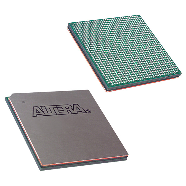
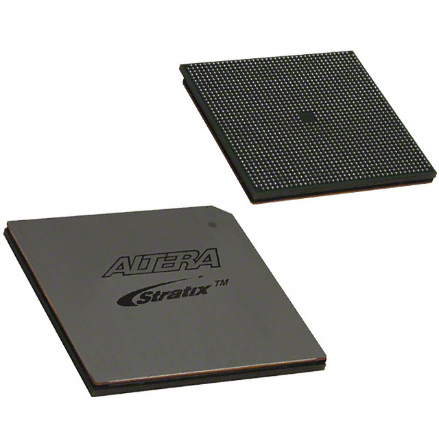
EP2S180F1020I4N
| Part Description |
Stratix® II Field Programmable Gate Array (FPGA) IC 742 9383040 179400 1020-BBGA |
|---|---|
| Quantity | 1,294 Available (as of June 10, 2026) |

| Product Category | Field Programmable Gate Array (FPGA) |
|---|---|
| Manufacturer | Intel |
| Manufacturing Status | Obsolete |
| Manufacturer Standard Lead Time | Contact Us |
| Datasheet |
Specifications & Environmental
| Device Package | 1020-FBGA (33x33) | Grade | Industrial | Operating Temperature | -40°C – 100°C | ||
|---|---|---|---|---|---|---|---|
| Package / Case | 1020-BBGA | Number of I/O | 742 | Voltage | 1.15 V - 1.25 V | ||
| Mounting Method | Surface Mount | RoHS Compliance | RoHS Compliant | REACH Compliance | REACH Unaffected | ||
| Moisture Sensitivity Level | 3 (168 Hours) | Number of LABs/CLBs | 8970 | Number of Logic Elements/Cells | 179400 | ||
| Number of Gates | N/A | ECCN | 3A001A7A | HTS Code | 8542.39.0001 | ||
| Qualification | N/A | Total RAM Bits | 9383040 |
Overview of EP2S180F1020I4N – Stratix II FPGA 1020-BBGA
The EP2S180F1020I4N is a Stratix® II Field Programmable Gate Array (FPGA) IC from Intel, delivered in a 1020-BBGA surface-mount package. It provides a high-capacity programmable fabric with 179,400 logic elements and 8,970 logic array blocks (LABs), plus extensive on-chip resources for complex digital designs.
Designed for industrial-grade applications, the device includes approximately 9.38 Mbits of embedded memory and 742 I/O pins, operates from a 1.15 V to 1.25 V core supply, and supports an operating temperature range of −40 °C to 100 °C. The Stratix II family handbook and device datasheet enumerate the FPGA’s architecture and configuration features for system integration and development.
Key Features
- Core Capacity 179,400 logic elements and 8,970 logic array blocks (LABs) provide the programmable fabric needed for large, complex designs.
- Embedded Memory Approximately 9.38 Mbits of on-chip RAM for packet buffers, FIFOs, and intermediate storage within custom datapaths.
- I/O Density 742 I/O pins delivered in a 1020-BBGA (supplier package 1020-FBGA, 33×33) footprint for rich peripheral and bus connectivity.
- Clocking & DSP Device handbook describes enhanced and fast PLLs, global and hierarchical clocking, and DSP block interfaces for high-performance timing and signal processing tasks.
- Advanced I/O Support Documentation covers double data rate I/O, high-speed differential I/O, programmable drive strength, on‑chip termination, and multi-voltage I/O interfacing.
- Configuration & Debug Includes IEEE 1149.1 JTAG boundary-scan support and SignalTap II embedded logic analyzer capability as detailed in the Stratix II handbook.
- Power & Mounting Surface-mount package with a core voltage supply range of 1.15 V to 1.25 V and specifications for hot-socketing and power-on reset in the device documentation.
- Industrial Grade & Compliance Specified operating temperature range of −40 °C to 100 °C and RoHS compliance for industrial deployments.
Typical Applications
- High‑performance signal processing: Use the DSP block interface and embedded memory to implement filtering, transforms, and real‑time data paths.
- High‑speed memory interfaces: The device supports external RAM interfacing and on‑chip memory structures for complex memory controller designs.
- Complex digital systems & prototyping: Large logic capacity and abundant I/O make the FPGA suitable for system prototyping, protocol bridging, and custom logic consolidation.
- Industrial control & automation: Industrial temperature rating and robust I/O support enable deployment in factory automation, motion control, and process control equipment.
Unique Advantages
- High logic capacity: 179,400 logic elements reduce the need for multi‑chip implementations and simplify system design integration.
- Substantial embedded memory: Approximately 9.38 Mbits of on‑chip RAM supports large buffers and local data storage for latency‑sensitive applications.
- Extensive I/O count: 742 I/Os in a 1020‑BBGA package provides flexibility for parallel interfaces, memory buses, and mixed‑signal front ends.
- Deterministic temperature range: Specified operation from −40 °C to 100 °C aligns with industrial deployment and reliability expectations.
- Configurable clocking and DSP support: Built‑in PLLs, hierarchical clocking, and DSP block interfaces in the Stratix II architecture facilitate high‑speed, low‑jitter designs.
- Standards and debug support: JTAG boundary‑scan and embedded logic analyzer features documented for the family streamline validation and production testing.
Why Choose EP2S180F1020I4N?
The EP2S180F1020I4N combines large logic capacity, substantial embedded memory, and broad I/O resources in a compact 1020‑BBGA footprint well suited for complex digital and industrial designs. With core documentation provided in the Stratix II device handbook, designers gain access to detailed architectural guidance covering memory, DSP, clock networks, and configuration options.
This device is positioned for projects that require high integration, deterministic industrial operation, and a documented architecture for advanced timing, I/O, and signal processing implementations. It is a practical choice for engineering teams building scalable, performance‑oriented FPGA solutions backed by Intel’s Stratix II family documentation.
Request a quote or submit a sourcing inquiry to obtain pricing, availability, and additional technical support for the EP2S180F1020I4N.


Date Founded: 1968
Headquarters: Santa Clara, California, USA
Employees: 130,000+
Revenue: $54.23 Billion
Certifications and Memberships: ISO9001:2015, ISO14001:2015, ISO17025:2017, ISO27001:2022, ISO45001:2018, ISO50001:2018


