
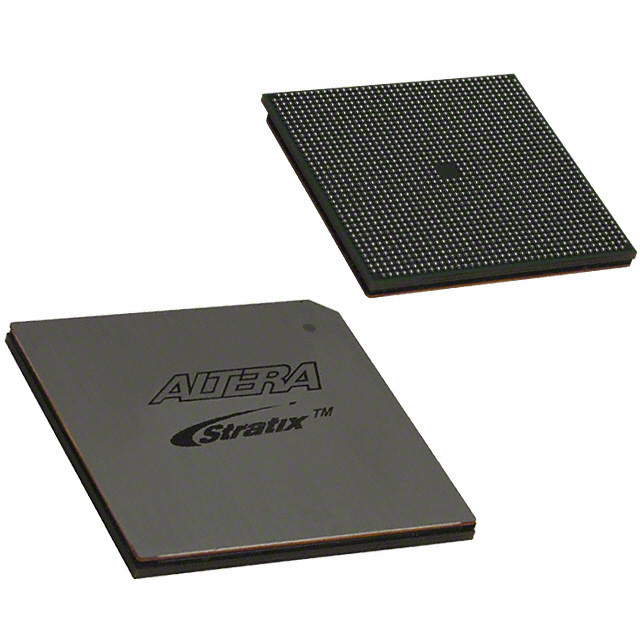
EP2S180F1508C3N
| Part Description |
Stratix® II Field Programmable Gate Array (FPGA) IC 1170 9383040 179400 1508-BBGA, FCBGA |
|---|---|
| Quantity | 809 Available (as of June 15, 2026) |
| Product Category | Field Programmable Gate Array (FPGA) |
|---|---|
| Manufacturer | Intel |
| Manufacturing Status | Obsolete |
| Manufacturer Standard Lead Time | Contact Us |
| Datasheet |
Specifications & Environmental
| Device Package | 1508-FBGA, FC (40x40) | Grade | Commercial | Operating Temperature | 0°C – 85°C | ||
|---|---|---|---|---|---|---|---|
| Package / Case | 1508-BBGA, FCBGA | Number of I/O | 1170 | Voltage | 1.15 V - 1.25 V | ||
| Mounting Method | Surface Mount | RoHS Compliance | RoHS Compliant | REACH Compliance | REACH Unaffected | ||
| Moisture Sensitivity Level | 3 (168 Hours) | Number of LABs/CLBs | 8970 | Number of Logic Elements/Cells | 179400 | ||
| Number of Gates | N/A | ECCN | 3A001A7A | HTS Code | 8542.39.0001 | ||
| Qualification | N/A | Total RAM Bits | 9383040 |
Overview of EP2S180F1508C3N – Stratix® II FPGA, 179,400 logic elements
The EP2S180F1508C3N is a Stratix® II Field Programmable Gate Array (FPGA) IC delivering a large programmable fabric for high‑density logic and system integration. It combines abundant logic resources, on‑chip memory, and extensive I/O to support complex digital designs.
Designed for applications that require significant logic capacity, memory bandwidth, and flexible I/O, this device targets systems that benefit from integrated DSP, clocking and memory interfacing capabilities while operating within commercial temperature ranges.
Key Features
- Logic Capacity — 8,970 LABs providing a total of 179,400 logic elements for implementing large FPGA designs and complex state machines.
- Embedded Memory — Approximately 9.38 Mbits of on‑chip RAM organized with TriMatrix memory and memory block resources for local buffering, FIFOs, and table storage.
- I/O Resources — 1,170 I/O pins supporting high‑density external interfacing and high‑speed memory links, including double data rate I/O and advanced I/O standard support as described in the device handbook.
- DSP & Clocking — Dedicated digital signal processing block resources and enhanced/fast PLLs with hierarchical/global clock networks for flexible clock management and signal processing tasks.
- Configuration & Test — Built‑in support for IEEE 1149.1 JTAG boundary‑scan and an embedded logic analyzer capability for in‑system debug and programmable configuration schemes.
- Power and Voltage — Core voltage supply range of 1.15 V to 1.25 V with hot‑socketing and power‑on reset features described for controlled power sequencing.
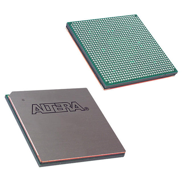
- Package & Mounting — 1508‑BBGA FCBGA package (supplier device package: 1508‑FBGA, FC 40×40) in a surface‑mount form factor for high‑density board integration.
- Operating Conditions & Compliance — Commercial grade device rated for 0 °C to 85 °C operation and RoHS compliant.
Typical Applications
- Digital Signal Processing — On‑chip DSP blocks and large logic fabric enable filtering, encoding/decoding and other compute‑intensive signal tasks.
- Memory Interface & Buffering — TriMatrix memory and abundant I/O are suited for external RAM interfacing and high‑bandwidth buffering applications.
- High‑Performance Embedded Systems — Use as a central programmable fabric to integrate control, peripheral interfacing, and custom logic in embedded platforms.
- High‑Speed I/O Designs — Extensive I/O count and advanced I/O support facilitate communication interfaces and parallel bus implementations.
Unique Advantages
- Highly Scalable Logic: 179,400 logic elements across 8,970 LABs lets designers scale complex logic without external glue logic.
- Significant On‑Chip Memory: Approximately 9.38 Mbits of embedded RAM reduces external memory dependence and simplifies board routing.
- Extensive I/O Capability: 1,170 I/Os provide the pin count needed for wide parallel buses, multiple interfaces, and high‑density connectors.
- Integrated DSP and Clocking: Dedicated DSP blocks and enhanced PLL networks streamline implementation of timing‑sensitive and signal‑processing functions.
- Compact High‑Density Package: 1508‑BBGA FCBGA packaging delivers large resource counts in a space‑efficient surface‑mount footprint.
- Commercial Temperature and RoHS Compliance: Rated for 0 °C to 85 °C operation and RoHS compliant for regulatory and manufacturing consistency.
Why Choose EP2S180F1508C3N?
The EP2S180F1508C3N combines a high logic element count, substantial embedded memory, and broad I/O capacity in a compact FCBGA package, making it well suited for designers who need to consolidate complex digital functions into a single programmable device. Its built‑in DSP resources, flexible clocking architecture and configuration/test features support advanced designs that require deterministic timing and in‑system debug.
This device is appropriate for teams building high‑density FPGA solutions within commercial temperature ranges that require a balance of logic, memory and I/O integration, with the long‑term benefit of a programmable platform for iterative development and system upgrades.
Request a quote or submit a pricing inquiry to receive availability and ordering information for EP2S180F1508C3N.


Date Founded: 1968
Headquarters: Santa Clara, California, USA
Employees: 130,000+
Revenue: $54.23 Billion
Certifications and Memberships: ISO9001:2015, ISO14001:2015, ISO17025:2017, ISO27001:2022, ISO45001:2018, ISO50001:2018


