
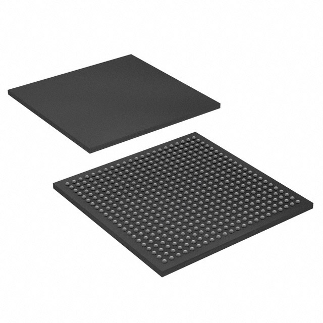
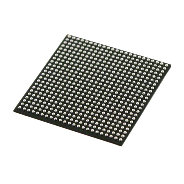
EP3C40U484C8N
| Part Description |
Cyclone® III Field Programmable Gate Array (FPGA) IC 331 1161216 39600 484-FBGA |
|---|---|
| Quantity | 1,516 Available (as of June 14, 2026) |

| Product Category | Field Programmable Gate Array (FPGA) |
|---|---|
| Manufacturer | Intel |
| Manufacturing Status | Active |
| Manufacturer Standard Lead Time | 26 Weeks |
| Datasheet |
Specifications & Environmental
| Device Package | 484-UBGA (19x19) | Grade | Commercial | Operating Temperature | 0°C – 85°C | ||
|---|---|---|---|---|---|---|---|
| Package / Case | 484-FBGA | Number of I/O | 331 | Voltage | 1.15 V - 1.25 V | ||
| Mounting Method | Surface Mount | RoHS Compliance | RoHS Compliant | REACH Compliance | REACH Unaffected | ||
| Moisture Sensitivity Level | 3 (168 Hours) | Number of LABs/CLBs | 2475 | Number of Logic Elements/Cells | 39600 | ||
| Number of Gates | N/A | ECCN | 3A991D | HTS Code | 8542.39.0001 | ||
| Qualification | N/A | Total RAM Bits | 1161216 |
Overview of EP3C40U484C8N – Cyclone® III FPGA, 39,600 logic elements, 484-FBGA
The EP3C40U484C8N is a Cyclone® III family field programmable gate array (FPGA) in a 484-FBGA package designed for commercial-grade applications. It integrates 39,600 logic elements, approximately 1.16 Mbits of embedded memory, and 331 user I/Os to address high-density logic, moderate embedded memory, and rich I/O requirements.
Built on the Cyclone III device family architecture, this device targets high-volume, low-power, and cost-sensitive markets where on-chip integration, flexible clocking, and diverse I/O support improve system-level design efficiency.
Key Features
- Logic Capacity — 39,600 logic elements provide substantial combinational and sequential resources for mid-range FPGA designs.
- Embedded Memory — Approximately 1.16 Mbits of on-chip RAM for buffering, FIFOs, and data storage close to logic.
- I/O Resources — 331 user I/Os to support broad connectivity and multiple interface domains on a single device.
- Clock Management — Cyclone III family architecture includes up to four PLLs per device with five outputs each for flexible clock synthesis and phase control.
- Package & Mounting — 484-FBGA (484-UBGA, 19×19) surface-mount package suitable for dense PCB layouts.
- Supply & Temperature — Core voltage range of 1.15 V to 1.25 V and commercial operating temperature range of 0 °C to 85 °C.
- Low-Power Family Architecture — Cyclone III family emphasizes low power through process and architecture choices to support thermally constrained designs and extended battery life in portable applications.
- I/O Standards & Signal Integrity — Family-level support for a wide range of I/O standards and adjustable slew rates, plus features such as on-chip termination calibration to address PVT variations.
- Compliance — RoHS compliant.
Typical Applications
- Portable and Handheld Devices — Low-power family architecture and compact 484-FBGA package make the device suitable for battery-powered and space-constrained systems.
- Consumer and Industrial Controls — Abundant logic elements, embedded memory, and 331 I/Os enable motor control, sensor aggregation, and user-interface management.
- Communications and I/O Bridging — Multiple I/Os and flexible clocking fit protocol bridging, I/O expansion, and interface consolidation tasks.
- Embedded System Integration — On-chip RAM, clock management, and family support for embedded processors (Nios II on the family) allow tight integration of control and data-path logic.
Unique Advantages
- Substantial Logic Density: 39,600 logic elements enable implementation of mid-range logic designs without external glue logic, reducing board complexity.
- High I/O Count: 331 user I/Os allow direct connection to multiple peripherals and high-pin-count interfaces, minimizing the need for external I/O expanders.
- Integrated Memory: Approximately 1.16 Mbits of embedded RAM keeps data paths on-chip for lower latency and simpler PCB routing.
- Flexible Clocking: Up to four PLLs with multiple outputs provide on-chip clock synthesis and phase control to simplify timing architectures.
- Commercial Temperature and RoHS Compliance: 0 °C to 85 °C rating with RoHS compliance supports mainstream commercial production and environmental requirements.
- Compact, Surface-Mount Packaging: 484-FBGA (19×19) package balances pin count and board area for dense, manufacturable designs.
Why Choose EP3C40U484C8N?
The EP3C40U484C8N positions itself as a practical, mid-range Cyclone III FPGA option where logic capacity, moderate embedded memory, and extensive I/O are required in a compact, commercial-grade device. Its family-level low-power architecture and on-chip clocking resources make it well suited to designs that demand integration and power-conscious operation.
Designers targeting high-volume or cost-sensitive products will appreciate the balance of logic, memory, and I/O in a RoHS-compliant 484-FBGA package, supported by the Cyclone III device family architecture and tool ecosystem.
Request a quote or submit an inquiry to receive pricing and availability for EP3C40U484C8N and to discuss how it fits your next design.


Date Founded: 1968
Headquarters: Santa Clara, California, USA
Employees: 130,000+
Revenue: $54.23 Billion
Certifications and Memberships: ISO9001:2015, ISO14001:2015, ISO17025:2017, ISO27001:2022, ISO45001:2018, ISO50001:2018


