
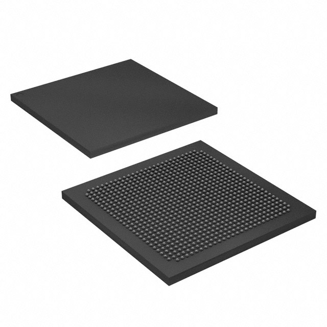
EP4SE360H29C3G
| Part Description |
Field Programmable Gate Array (FPGA) IC |
|---|---|
| Quantity | 227 Available (as of October 8, 2026) |
| Product Category | Field Programmable Gate Array (FPGA) |
|---|---|
| Manufacturer | Intel |
| Manufacturing Status | Active |
| Manufacturer Standard Lead Time | 8 Weeks |
| Datasheet |
Specifications & Environmental
| Device Package | 780-HBGA (33x33) | Grade | Commercial | Operating Temperature | 0°C – 85°C | ||
|---|---|---|---|---|---|---|---|
| Package / Case | 780-BBGA, FCBGA | Number of I/O | 488 | Voltage | 870 mV - 930 mV | ||
| Mounting Method | Surface Mount | RoHS Compliance | RoHS Compliant | REACH Compliance | REACH Unaffected | ||
| Moisture Sensitivity Level | 3 (168 Hours) | Number of LABs/CLBs | 14144 | Number of Logic Elements/Cells | 353600 | ||
| Number of Gates | N/A | ECCN | N/A | HTS Code | N/A | ||
| Qualification | N/A | Total RAM Bits | 23105536 |
Overview of EP4SE360H29C3G – Field Programmable Gate Array (FPGA) IC
The EP4SE360H29C3G is an Intel Stratix IV family FPGA configured as a high-capacity, reprogrammable logic device. It combines a large logic fabric, substantial on-chip memory, and a high I/O count to address demanding digital signal processing, high-bandwidth interfacing, and custom compute tasks.
Designed for commercial applications, this surface-mount FCBGA package delivers integration and flexibility for system designs that require significant programmable logic resources, wide protocol support as described in the Stratix IV device handbook, and features such as embedded memory and DSP blocks.
Key Features
- Logic Capacity — Approximately 353,600 logic elements provide broad room for complex designs, algorithm implementation, and custom datapaths.
- Embedded Memory — Approximately 23.1 Mbits of on-chip RAM support large buffering, FIFOs, and memory-mapped structures for high-throughput designs.
- I/O and Connectivity — 488 user I/O pins enable extensive peripheral and bus interfacing; the Stratix IV handbook highlights high-speed differential I/O and transceiver features for protocol flexibility.
- DSP and Processing Blocks — The Stratix IV family documentation references dedicated digital signal processing blocks suitable for compute- and throughput-intensive algorithms.
- Clocking and PLLs — Device handbook references integrated clock networks and PLLs to support complex timing architectures and multi-clock domains.
- Power Supply — Supported core voltage range is 870 mV to 930 mV, enabling defined power-domain design and supply selection.
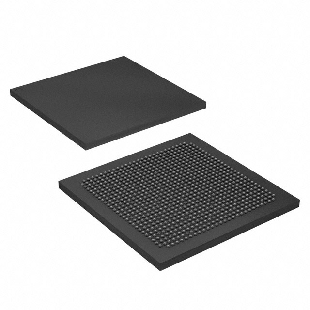
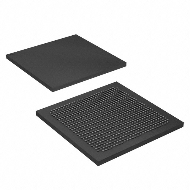
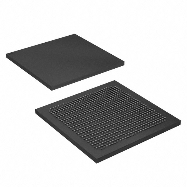
- Package & Mounting — Supplied in a 780-ball BGA (780-BBGA, FCBGA) / supplier device package 780-HBGA (33x33) for surface-mount assembly.
- Commercial Grade & Temperature — Rated for commercial-grade operation with an operating temperature range of 0 °C to 85 °C.
- Compliance — RoHS compliant to support environmentally regulated manufacturing flows.
Typical Applications
- High-bandwidth communications — Leverage the Stratix IV high-speed I/O and transceiver capabilities for protocol handling and aggregate data throughput tasks.
- Signal processing and DSP acceleration — Use on-chip DSP blocks and abundant logic elements to implement filters, transforms, and real-time processing pipelines.
- External memory interfaces — Combine the device’s embedded memory and I/O resources to implement memory controllers and buffering for external memory subsystems.
- Custom compute and control — Deploy large programmable logic capacity for hardware-accelerated algorithms, protocol offload, and system control functions.
Unique Advantages
- Large programmable fabric: Approximately 353,600 logic elements enable complex custom logic implementations and high-density designs.
- Substantial on-chip memory: Approximately 23.1 Mbits of embedded RAM reduce external memory dependency and simplify high-throughput buffering.
- High I/O count: 488 I/O pins support diverse peripheral connectivity and multi-channel interfaces.
- Stratix IV architecture features: Family-level features in the device handbook—such as advanced clock networks, PLLs, DSP blocks, and high-speed I/O—support demanding timing and protocol requirements.
- Commercial-grade compatibility: 0 °C to 85 °C operating range and RoHS compliance align with mainstream electronics manufacturing and assembly processes.
- FCBGA packaging for system integration: 780-ball FCBGA / 780-HBGA (33x33) package provides a compact surface-mount footprint for board-level integration.
Why Choose EP4SE360H29C3G?
The EP4SE360H29C3G delivers a high-capacity Stratix IV FPGA platform that balances large logic resources, significant embedded memory, and extensive I/O to support compute- and bandwidth-intensive designs. Its documented family features—such as advanced clocking, DSP blocks, and high-speed I/O—allow engineers to implement complex, multi-domain systems within a single programmable device.
This commercial-grade, RoHS-compliant FPGA in a 780-ball FCBGA package is suited to design teams and OEMs building high-throughput communications equipment, signal-processing subsystems, and custom hardware accelerators that require scalable logic density and flexible interfacing options.
Request a quote or submit an inquiry to purchase the EP4SE360H29C3G and discuss availability and volume pricing for your next design.






















Date Founded: 1968
Headquarters: Santa Clara, California, USA
Employees: 130,000+
Revenue: $54.23 Billion
Certifications and Memberships: ISO9001:2015, ISO14001:2015, ISO17025:2017, ISO27001:2022, ISO45001:2018, ISO50001:2018


