
EP4SGX70DF29C2XG
| Part Description |
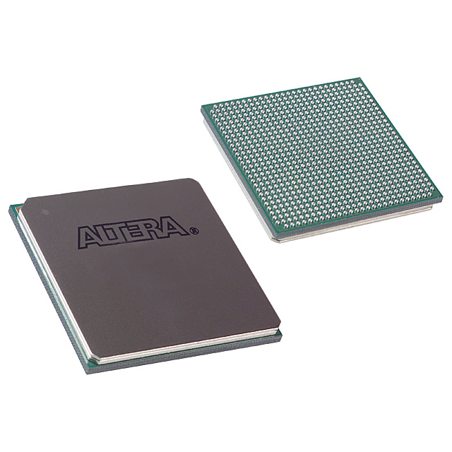
Stratix® IV GX Field Programmable Gate Array (FPGA) IC 372 7564880 72600 780-BBGA, FCBGA |
|---|---|
| Quantity | 353 Available (as of October 7, 2026) |

| Product Category | Field Programmable Gate Array (FPGA) |
|---|---|
| Manufacturer | Intel |
| Manufacturing Status | Active |
| Manufacturer Standard Lead Time | 26 Weeks |
| Datasheet |
Specifications & Environmental
| Device Package | 780-FBGA (29x29) | Grade | Commercial | Operating Temperature | 0°C – 85°C | ||
|---|---|---|---|---|---|---|---|
| Package / Case | 780-BBGA, FCBGA | Number of I/O | 372 | Voltage | 870 mV - 930 mV | ||
| Mounting Method | Surface Mount | RoHS Compliance | RoHS Compliant | REACH Compliance | REACH Unaffected | ||
| Moisture Sensitivity Level | 3 (168 Hours) | Number of LABs/CLBs | 2904 | Number of Logic Elements/Cells | 72600 | ||
| Number of Gates | N/A | ECCN | PENDING ECCN | HTS Code | 0000.00.0000 | ||
| Qualification | N/A | Total RAM Bits | 7564880 |
Overview of EP4SGX70DF29C2XG – Stratix® IV GX Field Programmable Gate Array (FPGA) IC
The EP4SGX70DF29C2XG is a Stratix IV GX family FPGA in a 780-BBGA (29×29) FCBGA package designed for high-bandwidth, system-level applications. It provides a programmable fabric with 72,600 logic elements and architecture features described for Stratix IV GX devices, targeting designs that require dense logic, substantial on-chip memory, and advanced I/O capabilities.
This commercial-grade device is suited for applications demanding high aggregate data bandwidth and flexible protocol support, delivering a combination of logic capacity, embedded memory, and I/O resources with defined supply and temperature ranges for predictable system integration.
Key Features
- FPGA Core Stratix IV GX architecture with 72,600 logic elements for complex, programmable digital logic implementations.
- Embedded Memory Approximately 7.56 Mbits of on-chip RAM to support packet buffering, frame memory, and intermediate DSP storage.
- High-Speed Transceiver and I/O Family-level support for high-speed transceiver features and high aggregate data bandwidth; device provides 372 I/O pins for extensive external interfacing.
- DSP and System Features Architecture includes support for digital signal processing blocks and system integration features such as PLLs and robust clock networks.
- Package and Mounting 780-BBGA (FCBGA) supplier device package 780-FBGA (29×29), surface-mount packaging optimized for board-level integration.
- Power and Electrical Core voltage supply specified from 870 mV to 930 mV for defined power domain planning.
- Operating Conditions and Compliance Commercial grade operation from 0 °C to 85 °C and RoHS-compliant for regulatory alignment.
- Diagnostics and Signal Integrity Series documentation highlights diagnostic features and signal integrity capabilities useful for high-performance designs.
Typical Applications
- High-Speed Networking and Telecommunications — Implements protocol processing and packet handling where high aggregate bandwidth and high-speed transceivers are required.
- High-Performance Signal Processing — Uses on-chip DSP resources and embedded RAM for video processing, modulation/demodulation, and real-time analytics.
- Memory-Intensive Interfaces — Acts as a bridge or controller for external memory interfaces and system-level data buffering leveraging the device’s embedded memory.
- System Integration and Test Equipment — Leverages extensive I/O and diagnostic capabilities for complex prototyping, instrumentation, and measurement systems.
Unique Advantages
- High Logic Density: 72,600 logic elements provide substantial capacity for complex state machines, custom processors, and hardware accelerators, reducing the need for multiple devices.
- Significant On-Chip Memory: Approximately 7.56 Mbits of embedded RAM supports large buffers and intermediate data storage without relying solely on external memory.
- Extensive I/O Count: 372 I/O pins enable broad system connectivity and flexible partitioning of interfaces across the board.
- Family-Level High-Speed Features: Stratix IV GX series characteristics (high-speed transceivers, clocking resources, diagnostic features) align the device to high-throughput and protocol-diverse designs.
- Board-Level Packaging: 780-FBGA (29×29) surface-mount package simplifies mechanical integration for dense PCBs and controlled impedance routing.
- Predictable Operating Envelope: Commercial grade temperature range (0 °C to 85 °C) and defined core voltage range (870–930 mV) support repeatable design margins and power planning.
Why Choose EP4SGX70DF29C2XG?
The EP4SGX70DF29C2XG combines Stratix IV GX family architecture with high logic capacity, substantial embedded memory, and a large I/O complement to address demanding data-path and system-integration tasks. Its documented family features—high-speed transceivers, DSP support, and comprehensive clocking and diagnostic resources—make it a suitable choice for designs that require a balance of performance, integration, and predictable operating characteristics.
This device is well matched to engineering teams developing high-bandwidth communications, advanced signal-processing modules, and complex system controllers that benefit from an FPGA with strong on-chip memory and extensive interfacing options. Its commercial-grade rating and RoHS compliance support deployment in mainstream electronic systems with standard environmental profiles.
To request pricing or a formal quote for EP4SGX70DF29C2XG, submit an inquiry with the part number and your quantity and delivery requirements.

























Date Founded: 1968
Headquarters: Santa Clara, California, USA
Employees: 130,000+
Revenue: $54.23 Billion
Certifications and Memberships: ISO9001:2015, ISO14001:2015, ISO17025:2017, ISO27001:2022, ISO45001:2018, ISO50001:2018


