
EPF10K20RC240-3
| Part Description |
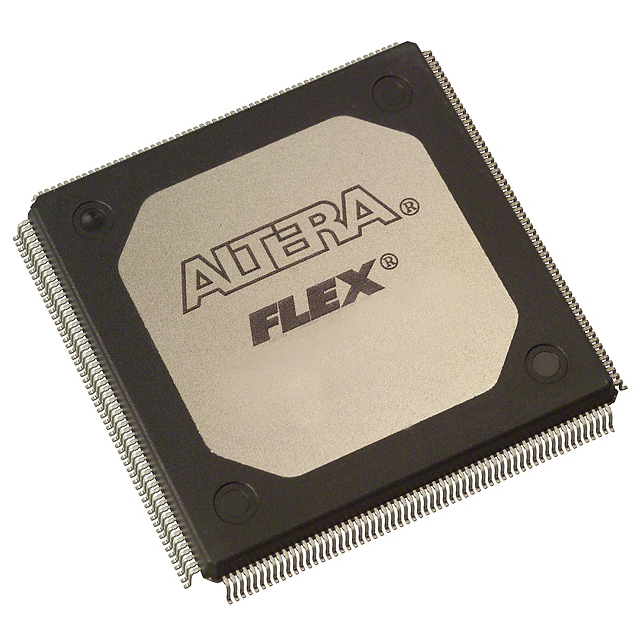
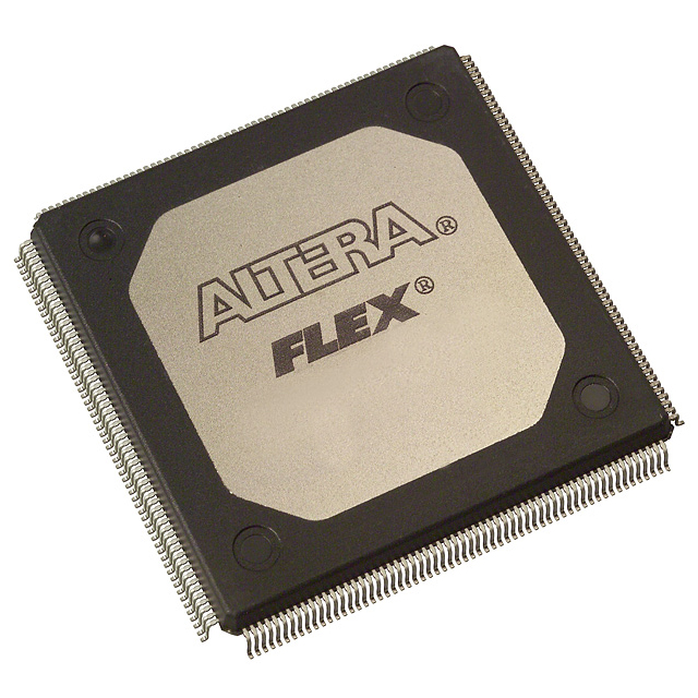
FLEX-10K® Field Programmable Gate Array (FPGA) IC 189 12288 1152 240-BFQFP Exposed Pad |
|---|---|
| Quantity | 1,154 Available (as of October 7, 2026) |
| Product Category | Field Programmable Gate Array (FPGA) |
|---|---|
| Manufacturer | Intel |
| Manufacturing Status | Obsolete |
| Manufacturer Standard Lead Time | Contact Us |
| Datasheet |
Specifications & Environmental
| Device Package | 240-RQFP (32x32) | Grade | Commercial | Operating Temperature | 0°C – 70°C | ||
|---|---|---|---|---|---|---|---|
| Package / Case | 240-BFQFP Exposed Pad | Number of I/O | 189 | Voltage | 4.75 V - 5.25 V | ||
| Mounting Method | Surface Mount | RoHS Compliance | RoHS non-compliant | REACH Compliance | REACH Unaffected | ||
| Moisture Sensitivity Level | 3 (168 Hours) | Number of LABs/CLBs | 144 | Number of Logic Elements/Cells | 1152 | ||
| Number of Gates | 63000 | ECCN | 3A991D | HTS Code | 8542.39.0001 | ||
| Qualification | N/A | Total RAM Bits | 12288 |
Overview of EPF10K20RC240-3 – FLEX-10K FPGA, 1,152 logic elements, 12,288 RAM bits, 189 I/O, 240-BFQFP
The EPF10K20RC240-3 is an Intel FLEX-10K family field programmable gate array (FPGA) in a 240-BFQFP exposed pad package. It pairs a dedicated logic array with embedded memory resources to implement programmable logic and megafunctions for commercial embedded designs.
With 1,152 logic elements, 12,288 bits of on-chip RAM and 189 user I/O pins, this device targets designs that require moderate logic density, significant on-chip memory and a high pin-count footprint while operating from a 5.0 V supply range.
Key Features
- Embedded programmable logic architecture System-on-a‑programmable‑chip (SOPC) family architecture with separate embedded array and logic array to implement megafunctions and general logic functions.
- Logic capacity 1,152 logic elements (LEs) providing the programmable logic resource for mid-density designs.
- On-chip memory Approximately 12,288 bits of embedded RAM distributed across the device for efficient implementation of FIFOs, buffers and small data stores.
- I/O and routing 189 user I/O pins to support complex interfacing; FastTrack® continuous routing structure and dedicated carry/cascade chains for predictable, high-speed logic paths (family feature).
- Supply and thermal Designed for 5.0 V operation with a specified voltage range of 4.75 V to 5.25 V and a commercial operating temperature range of 0 °C to 70 °C.
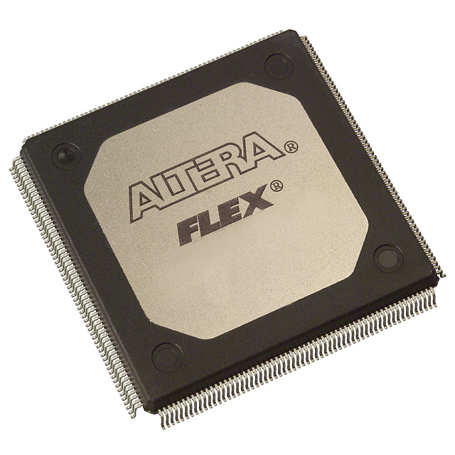
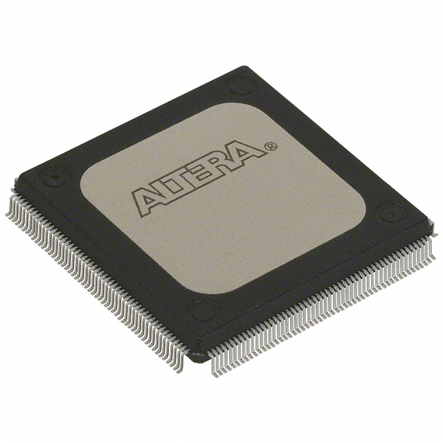
- Package and mounting 240-BFQFP exposed pad surface-mount package (supplier package: 240-RQFP, 32×32) for dense PCB layout with thermal pad support.
- Programming and test Family features include in-circuit reconfigurability (ICR) via external configuration device or JTAG and IEEE 1149.1 boundary-scan test circuitry (family feature).
- Regulatory and handling RoHS compliant and supplied as a surface-mount commercial-grade device.
Typical Applications
- Embedded system integration Implement SOPC-style integration and custom control logic where moderate logic density and on-chip RAM are required.
- Interface and I/O aggregation Use the device’s 189 I/O pins to consolidate multiple peripheral interfaces or bridge between logic domains on a single chip.
- Memory‑aware logic blocks Deploy the 12,288 bits of embedded RAM for small buffering, lookup tables or temporary data storage within programmable logic.
- Prototyping and commercial products Commercial-grade designs that need field-programmable flexibility, reconfigurability and a high-pin-count packaged device.
Unique Advantages
- Balanced logic and memory resources: 1,152 logic elements paired with 12,288 bits of embedded RAM enables combined logic-plus-memory megafunctions without external memory in many designs.
- High I/O count: 189 user I/O pins support complex board-level integration and multiple peripheral connections from a single device.
- 5.0 V supply compatibility: Specified 4.75 V to 5.25 V operation simplifies integration into 5 V commercial platforms.
- In-system programmability and testability: Family-level support for in-circuit reconfiguration and IEEE 1149.1 JTAG boundary-scan test facilitates development and manufacturing test flows.
- Thermal-friendly package: 240-BFQFP with exposed pad supports PCB thermal management while keeping a compact footprint.
- RoHS compliant commercial part: Meets RoHS environmental requirements for commercial electronics production.
Why Choose EPF10K20RC240-3?
The EPF10K20RC240-3 delivers a mid-density FLEX-10K FPGA solution that combines 1,152 logic elements, substantial embedded RAM and an extensive I/O count in a 240-pin exposed-pad package. It is well suited for commercial embedded applications that require reconfigurable logic, on-chip memory and a high number of external interfaces while operating on a 5.0 V supply.
This device appeals to designers who need a programmable, testable and RoHS-compliant FPGA option for consolidating logic functions, implementing megafunctions and simplifying board-level integration with in-system reconfigurability and boundary-scan support.
Request a quote or submit a technical inquiry to receive pricing, availability and lead-time information for the EPF10K20RC240-3.
























Date Founded: 1968
Headquarters: Santa Clara, California, USA
Employees: 130,000+
Revenue: $54.23 Billion
Certifications and Memberships: ISO9001:2015, ISO14001:2015, ISO17025:2017, ISO27001:2022, ISO45001:2018, ISO50001:2018


