
EPF10K30EFC256-2N
| Part Description |
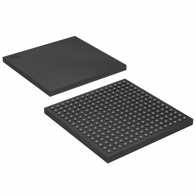
FLEX-10KE® Field Programmable Gate Array (FPGA) IC 176 24576 1728 256-BGA |
|---|---|
| Quantity | 711 Available (as of June 14, 2026) |
| Product Category | Field Programmable Gate Array (FPGA) |
|---|---|
| Manufacturer | Intel |
| Manufacturing Status | Obsolete |
| Manufacturer Standard Lead Time | Contact Us |
| Datasheet |
Specifications & Environmental
| Device Package | 256-FBGA (17x17) | Grade | Commercial | Operating Temperature | 0°C – 70°C | ||
|---|---|---|---|---|---|---|---|
| Package / Case | 256-BGA | Number of I/O | 176 | Voltage | 2.375 V - 2.625 V | ||
| Mounting Method | Surface Mount | RoHS Compliance | Unknown | REACH Compliance | REACH Unaffected | ||
| Moisture Sensitivity Level | 3 (168 Hours) | Number of LABs/CLBs | 216 | Number of Logic Elements/Cells | 1728 | ||
| Number of Gates | 119000 | ECCN | 3A001A2A | HTS Code | 8542.39.0001 | ||
| Qualification | N/A | Total RAM Bits | 24576 |
Overview of EPF10K30EFC256-2N – FLEX-10KE FPGA, 1728 Logic Elements, 256-FBGA
The EPF10K30EFC256-2N is a FLEX-10KE family field-programmable gate array (FPGA) offered by Intel. It provides 1,728 logic elements, 24,576 bits of embedded RAM, and 176 user I/O in a compact 256-FBGA (17×17) surface-mount package for commercial-grade embedded designs.
Designed for mid-density programmable logic tasks, this device targets applications that require on-chip memory, flexible I/O capacity, boundary-scan testability and field reconfigurability while operating within a 2.375–2.625 V supply range and 0 °C to 70 °C operating temperature.
Key Features
- Logic Capacity — 1,728 logic elements providing up to 119,000 gates of logic capacity as specified for the device.
- On-chip RAM — 24,576 bits of embedded RAM for implementing buffers, FIFOs and small data stores without external memory.
- I/O and Package — 176 user I/O pins in a 256-FBGA (17×17) surface-mount package optimized for dense board layouts.
- Power Supply — Specified operating supply range of 2.375 V to 2.625 V to match system power rails requiring this voltage window.
- Commercial Temperature Grade — Rated for 0 °C to 70 °C operation and RoHS-compliant for standard commercial deployments.
- Built-in Test & Configuration — Includes JTAG boundary-scan circuitry compliant with IEEE Std. 1149.1-1990 for device test and in-system programming without consuming user logic.
- Family Architecture Features — As a FLEX 10K family device, the architecture supports embedded array blocks for megafunctions, dedicated carry and cascade chains for arithmetic and high‑fan‑in logic, and low-skew clock distribution to aid predictable timing (family-level features described in the FLEX 10K datasheet).
Typical Applications
- Embedded Control & Glue Logic — Implement custom control logic, protocol bridging, and peripheral interfacing where flexible logic and moderate on-chip memory are required.
- Interface & I/O Expansion — Use the device’s 176 I/O pins for signal aggregation, buffering, and protocol adaptation between subsystems.
- Prototyping and System Integration — Field-programmable capability and JTAG support make it suitable for hardware validation and iterative development cycles.
- Signal Processing Primitives — Leverage dedicated carry and cascade chains for compact implementations of adders, counters, and comparators in embedded applications.
Unique Advantages
- Moderate logic density with on-chip memory: 1,728 logic elements combined with 24,576 bits of RAM reduces dependence on external memory for small buffers and control-state storage.
- High pin count in a compact package: 176 I/O in a 256-FBGA (17×17) package enables dense I/O routing while conserving board area.
- Field reconfigurability and testability: Built-in JTAG boundary-scan and in-circuit reconfigurability support system-level debugging and firmware updates without consuming user logic.
- Commercial-grade qualification and RoHS compliance: Device is specified for 0 °C to 70 °C operation and meets RoHS environmental requirements for mainstream product deployments.
- Architecture-level primitives: Family-level features such as dedicated carry/cascade chains and low-skew clock resources help simplify arithmetic and timing-critical logic implementations.
Why Choose EPF10K30EFC256-2N?
The EPF10K30EFC256-2N is positioned for engineers who need a mid-density, field-programmable solution with meaningful on-chip RAM and extensive I/O in a space-efficient BGA package. Its combination of 1,728 logic elements, 24,576 bits of embedded memory and 176 user I/O makes it well suited for embedded control, interface logic, and prototyping tasks where in-system configurability and board-level integration are priorities.
Backed by the FLEX 10K family datasheet and the associated development tool flow, this device offers an established architecture with features aimed at simplifying design implementation and board-level testing. Its commercial temperature rating and RoHS compliance support standard production deployments in mainstream embedded products.
Request a quote or submit a product inquiry for EPF10K30EFC256-2N to start procurement; please include the part number and any project requirements to expedite your request.


Date Founded: 1968
Headquarters: Santa Clara, California, USA
Employees: 130,000+
Revenue: $54.23 Billion
Certifications and Memberships: ISO9001:2015, ISO14001:2015, ISO17025:2017, ISO27001:2022, ISO45001:2018, ISO50001:2018


