
EPF10K30EFC256-2X
| Part Description |
FLEX-10KE® Field Programmable Gate Array (FPGA) IC 176 24576 1728 256-BGA |
|---|---|
| Quantity | 7 Available (as of October 8, 2026) |

| Product Category | Field Programmable Gate Array (FPGA) |
|---|---|
| Manufacturer | Intel |
| Manufacturing Status | Obsolete |
| Manufacturer Standard Lead Time | Contact Us |
| Datasheet |
Specifications & Environmental
| Device Package | 256-FBGA (17x17) | Grade | Commercial | Operating Temperature | 0°C – 70°C | ||
|---|---|---|---|---|---|---|---|
| Package / Case | 256-BGA | Number of I/O | 176 | Voltage | 2.375 V - 2.625 V | ||
| Mounting Method | Surface Mount | RoHS Compliance | Unknown | REACH Compliance | REACH Unaffected | ||
| Moisture Sensitivity Level | 3 (168 Hours) | Number of LABs/CLBs | 216 | Number of Logic Elements/Cells | 1728 | ||
| Number of Gates | 119000 | ECCN | 3A001A2A | HTS Code | 8542.39.0001 | ||
| Qualification | N/A | Total RAM Bits | 24576 |
Overview of EPF10K30EFC256-2X – FLEX-10KE Field Programmable Gate Array, 256‑BGA, 176 I/O
The EPF10K30EFC256-2X is a FLEX-10KE family Field Programmable Gate Array (FPGA) in a 256‑BGA package designed for embedded programmable logic applications. It combines a logic array and embedded memory to support System‑on‑a‑Programmable‑Chip (SOPC) integration and megafunction implementation.
With 1,728 logic elements, approximately 24,576 bits of on‑chip RAM, and 176 user I/O pins, this device targets medium-density embedded designs that require flexible I/O, in‑circuit reconfigurability, and compact board-level packaging.
Key Features
- Core Logic — 1,728 logic elements providing configurable logic resources for glue logic, state machines, and custom datapaths.
- On‑chip Memory — 24,576 total RAM bits of embedded memory for buffering, small FIFOs, and distributed storage close to logic.
- I/O Capacity — 176 user I/O pins suited for consolidating interfaces and supporting multiple peripheral connections on a single device.
- Gate Density — Approximately 119,000 gates to quantify overall implementation capacity for mixed logic and memory functions.
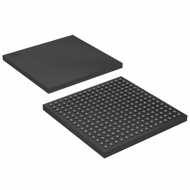
- Package & Mounting — 256‑BGA (256‑FBGA, 17×17) surface‑mount package for compact PCB integration and high pin density.
- Power & Supply — Supported supply voltage range of 2.375 V to 2.625 V to match system power rails and design constraints.
- Operating Range — Commercial operating temperature range of 0 °C to 70 °C for standard commercial applications.
- In‑Circuit Reconfigurability & Test — Series features include in‑circuit reconfigurability via external configuration devices or the JTAG port and built‑in IEEE 1149.1 JTAG boundary‑scan circuitry.
- Compliance — RoHS‑compliant for environmental and supply‑chain requirements.
Typical Applications
- Embedded Control — Implement control logic, protocol handling, and glue logic for compact embedded systems that need reprogrammability.
- Interface Bridging — Consolidate multiple parallel or serial interfaces using the device’s 176 I/O pins to reduce overall BOM and board complexity.
- Prototyping & Development — Rapidly iterate and validate custom logic functions and megafunctions during product development using in‑circuit reconfiguration.
- Memory‑Centered Functions — Use on‑chip RAM for buffering, small FIFOs, and fast local storage close to processing logic.
Unique Advantages
- Balanced Medium Density: 1,728 logic elements and ~119,000 gates provide a clear capacity point for medium‑complexity designs without overprovisioning.
- Substantial Embedded Memory: Approximately 24,576 bits of on‑chip RAM enable local data buffering and reduce the need for external memory in many applications.
- High I/O Count: 176 user I/O pins allow consolidation of peripherals and interfaces, simplifying board routing and reducing component count.
- Compact, High‑Pin‑Count Package: 256‑FBGA (17×17) package delivers high pin density in a small footprint for space‑constrained PCBs.
- Reconfigurability and Test Support: JTAG boundary‑scan and in‑circuit reconfigurability support production testing and field updates without consuming device logic.
- Regulatory Readiness: RoHS compliance supports modern environmental and manufacturing standards.
Why Choose EPF10K30EFC256-2X?
The EPF10K30EFC256-2X positions itself as a practical, medium‑density FPGA choice for designers who need a blend of logic resources, embedded memory, and a high I/O count in a compact BGA package. Its support for in‑circuit reconfigurability and JTAG boundary‑scan simplifies development cycles and production test flows.
This device suits teams building embedded controllers, interface bridging solutions, and prototype systems that benefit from on‑device memory and reprogrammability. Backed by FLEX‑10K family documentation and development tool support, it provides a predictable platform for iterative design and deployment.
Request a quote or submit an inquiry to receive pricing and availability information for the EPF10K30EFC256-2X. Our team can provide lead‑time details and support for your procurement needs.
























Date Founded: 1968
Headquarters: Santa Clara, California, USA
Employees: 130,000+
Revenue: $54.23 Billion
Certifications and Memberships: ISO9001:2015, ISO14001:2015, ISO17025:2017, ISO27001:2022, ISO45001:2018, ISO50001:2018


