
EPF10K30EFC256-2
| Part Description |
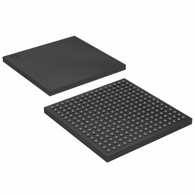
FLEX-10KE® Field Programmable Gate Array (FPGA) IC 176 24576 1728 256-BGA |
|---|---|
| Quantity | 218 Available (as of June 15, 2026) |

| Product Category | Field Programmable Gate Array (FPGA) |
|---|---|
| Manufacturer | Intel |
| Manufacturing Status | Obsolete |
| Manufacturer Standard Lead Time | Contact Us |
| Datasheet |
Specifications & Environmental
| Device Package | 256-FBGA (17x17) | Grade | Commercial | Operating Temperature | 0°C – 70°C | ||
|---|---|---|---|---|---|---|---|
| Package / Case | 256-BGA | Number of I/O | 176 | Voltage | 2.375 V - 2.625 V | ||
| Mounting Method | Surface Mount | RoHS Compliance | Unknown | REACH Compliance | REACH Unaffected | ||
| Moisture Sensitivity Level | 3 (168 Hours) | Number of LABs/CLBs | 216 | Number of Logic Elements/Cells | 1728 | ||
| Number of Gates | 119000 | ECCN | 3A001A2A | HTS Code | 8542.39.0001 | ||
| Qualification | N/A | Total RAM Bits | 24576 |
Overview of EPF10K30EFC256-2 – FLEX-10KE® Field Programmable Gate Array (FPGA) IC 176 24576 1728 256-BGA
The EPF10K30EFC256-2 is a FLEX-10KE embedded programmable logic device designed for mid-density FPGA applications. It combines a logic array and embedded resources to support System-on-a-Programmable-Chip (SOPC) integration, making it suitable for custom logic, buffering, and I/O-centric designs.
With 1,728 logic elements, 24,576 bits of on-chip RAM and 176 user I/O pins in a compact 256-FBGA (17×17) surface-mount package, the device targets commercial designs that require a balance of logic, embedded memory and flexible I/O connectivity within a commercial temperature range.
Key Features
- Logic Core 1,728 logic elements organized into 216 LABs provide the programmable fabric for custom combinational and sequential logic.
- Embedded Memory 24,576 bits of on-chip RAM for lookup tables, FIFOs and buffering without external memory.
- I/O Capacity 176 user I/O pins support a wide range of external interfaces and parallel connections for system integration.
- Package & Mounting 256-FBGA (17×17) surface-mount package (256-BGA) balances board-space efficiency with thermal characteristics for commercial assemblies.
- Power Supply Specified operating supply range of 2.375 V to 2.625 V for the device core and I/O as provided in the product data.
- Temperature & Grade Commercial grade device rated for 0 °C to 70 °C operation.
- Built-in Test & Configuration Includes IEEE 1149.1-compliant JTAG boundary-scan support for configuration and in-circuit test.
- Clock & Interconnect Features Architecture includes dedicated carry and cascade chains, low-skew clock distribution and multiple global clock/clear resources to support arithmetic, high-fan-in logic and synchronous designs.
- Environmental RoHS compliant.
Typical Applications
- Custom Control Logic Implement motor-control state machines, protocol handlers or application-specific controllers using the device’s logic elements and embedded RAM.
- Interface Bridging Use the 176 I/O pins to implement parallel interfaces, level translation buffering and glue logic between system components.
- Embedded Data Buffering On-chip RAM supports small FIFOs, lookup tables and temporary storage to reduce external memory dependencies.
- Prototyping and Development Mid-density programmable fabric provides a platform for iterative hardware development and system validation.
Unique Advantages
- Balanced Logic and Memory Density: 1,728 logic elements combined with 24,576 bits of embedded RAM delivers a practical mix of resources for mid-range designs.
- High I/O Count: 176 user I/O pins enable rich peripheral connectivity and flexible board-level integration.
- Compact BGA Package: 256-FBGA (17×17) package conserves PCB area while supporting surface-mount assembly.
- On-chip Test and Configuration: Built-in IEEE 1149.1 JTAG boundary-scan simplifies in-circuit test and configuration workflows.
- Clocking and Arithmetic Support: Dedicated carry and cascade chains plus low-skew clock distribution facilitate efficient implementation of adders, counters and high-speed logic structures.
- Regulatory Compliance: RoHS compliant for safer materials compliance in commercial products.
Why Choose EPF10K30EFC256-2?
The EPF10K30EFC256-2 positions itself as a versatile mid-density FPGA option for commercial electronic designs that need a balanced combination of logic, embedded RAM and a high I/O count in a compact surface-mount BGA. Its on-chip resources and architectural features support SOPC-style integration and common synchronous design patterns.
This device is well suited for engineers and product teams building interface logic, embedded controllers, data buffering or prototype systems where predictable integration, boundary-scan testability and a commercial operating temperature range are required.
Request a quote or submit an inquiry to obtain pricing and availability for the EPF10K30EFC256-2 and discuss lead times or volume requirements.


Date Founded: 1968
Headquarters: Santa Clara, California, USA
Employees: 130,000+
Revenue: $54.23 Billion
Certifications and Memberships: ISO9001:2015, ISO14001:2015, ISO17025:2017, ISO27001:2022, ISO45001:2018, ISO50001:2018


