
EPF10K40RC240-4
| Part Description |
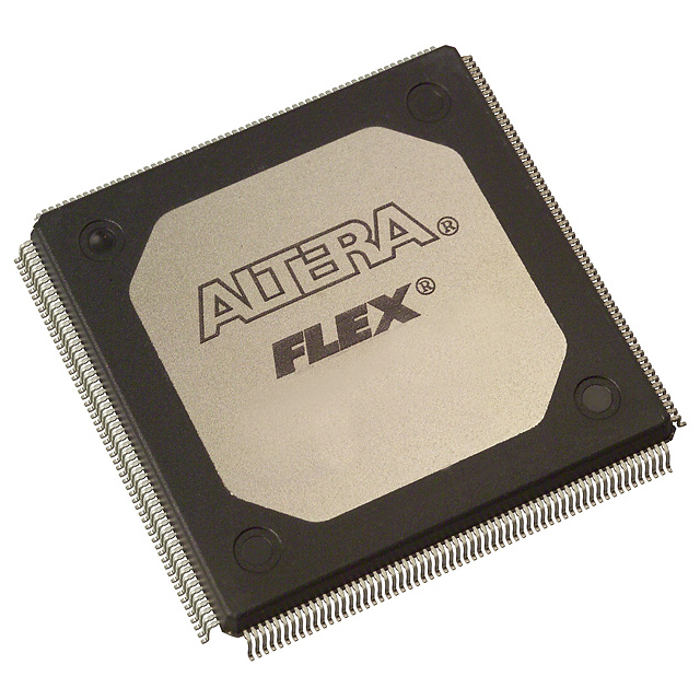
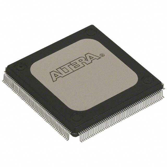
FLEX-10K® Field Programmable Gate Array (FPGA) IC 189 16384 2304 240-BFQFP Exposed Pad |
|---|---|
| Quantity | 1,097 Available (as of June 10, 2026) |

| Product Category | Field Programmable Gate Array (FPGA) |
|---|---|
| Manufacturer | Intel |
| Manufacturing Status | Obsolete |
| Manufacturer Standard Lead Time | Contact Us |
| Datasheet |
Specifications & Environmental
| Device Package | 240-RQFP (32x32) | Grade | Commercial | Operating Temperature | 0°C – 70°C | ||
|---|---|---|---|---|---|---|---|
| Package / Case | 240-BFQFP Exposed Pad | Number of I/O | 189 | Voltage | 4.75 V - 5.25 V | ||
| Mounting Method | Surface Mount | RoHS Compliance | RoHS non-compliant | REACH Compliance | REACH Unaffected | ||
| Moisture Sensitivity Level | 3 (168 Hours) | Number of LABs/CLBs | 288 | Number of Logic Elements/Cells | 2304 | ||
| Number of Gates | 93000 | ECCN | 3A991D | HTS Code | 8542.39.0001 | ||
| Qualification | N/A | Total RAM Bits | 16384 |
Overview of EPF10K40RC240-4 – FLEX-10K FPGA, 2,304 Logic Elements, 16,384 Bits RAM, 189 I/O, 240-BFQFP
The EPF10K40RC240-4 is a FLEX-10K family field-programmable gate array (FPGA) from Intel designed for commercial embedded logic applications. It combines a logic array and embedded memory to implement custom logic, on-chip megafunctions, and system-level integration in a single programmable device.
Targeted at commercial embedded designs that require moderate logic density and abundant I/O, this device delivers 2,304 logic elements, approximately 16,384 bits of embedded RAM, and up to 189 user I/O pins in a 240-BFQFP exposed-pad package, operating from a 4.75 V to 5.25 V supply and rated for 0 °C to 70 °C.
Key Features
- Logic Capacity — 2,304 logic elements and 288 logic array blocks (LABs) provide moderate-density programmable logic for custom combinational and sequential functions.
- Embedded Memory — Approximately 16,384 bits of on-chip RAM support storage for FIFOs, small tables, and megafunctions without reducing logic capacity.
- I/O and Interfacing — 189 user I/O pins enable dense external connectivity for buses, sensors, and peripherals in I/O-heavy designs.
- Gate Count — Listed system gates value of 93,000 for planning system-level capacity and partitioning.
- Supply and Power — Designed for 5.0-V class systems with a supply range of 4.75 V to 5.25 V.
- Packaging and Mounting — 240-BFQFP exposed pad (240-RQFP, 32×32) surface-mount package provides thermal dissipation options and board-level compatibility.
- Configuration and Test — Supports in-circuit reconfigurability via external configuration device, intelligent controller, or JTAG; includes built-in JTAG boundary-scan (IEEE Std. 1149.1) for board-level test access.
- Clock and Arithmetic Support — Family-level features include dedicated carry and cascade chains plus low-skew clock distribution to implement high-performance adders and wide logic efficiently.
- Commercial Temperature Range — Operates across 0 °C to 70 °C for commercial-grade applications.
- RoHS Compliant — Meets RoHS environmental requirements for lead-free assembly.
Typical Applications
- Embedded System Integration — Implement SOPC-style integration and custom logic blocks for commercial embedded products that require on-chip memory and configurable logic.
- Interface Bridging & Protocol Glue — Use the abundant I/O to bridge peripheral buses, adapt signal standards, and implement protocol translation in board-level designs.
- Control and Sequencing — Implement industrial control sequencing, state machines, and timing-critical control logic where deterministic programmable logic is required.
- High I/O Peripheral Management — Manage multiple sensors, displays, and user-interface peripherals using the device’s 189 I/O pins and embedded RAM for buffering.
Unique Advantages
- Balanced Logic and Memory — 2,304 logic elements paired with approximately 16,384 bits of embedded RAM enable mixed logic-plus-memory megafunctions without sacrificing logic capacity.
- High I/O Density — 189 user I/O pins allow compact designs that require many external connections, reducing the need for additional interface chips.
- Board-Ready Packaging — 240-BFQFP exposed-pad surface-mount package simplifies thermal management and supports common PCB assembly processes.
- In-Circuit Reconfigurability and Test — JTAG boundary-scan and multiple configuration options streamline development, programming, and board-level diagnostics.
- Commercial Deployment — Designed for commercial temperature ranges and RoHS-compliant production, suitable for mainstream embedded product lines.
Why Choose EPF10K40RC240-4?
The EPF10K40RC240-4 offers a practical balance of logic density, embedded memory, and I/O capability for commercial embedded designs that need on-chip megafunctions and flexible interfacing. As a member of the FLEX 10K family, it provides architecture-level features—such as dedicated arithmetic chains, configurable clock distribution, and multiple configuration paths—that simplify mapping common functions into programmable logic.
This device is well suited to engineers and product teams building commercial embedded systems that require moderate gate counts, substantial I/O, and on-board RAM, backed by the FLEX 10K family design resources and tool support referenced in the family datasheet.
Request a quote or submit a pricing inquiry for EPF10K40RC240-4 to check current availability and lead times for your next design.


Date Founded: 1968
Headquarters: Santa Clara, California, USA
Employees: 130,000+
Revenue: $54.23 Billion
Certifications and Memberships: ISO9001:2015, ISO14001:2015, ISO17025:2017, ISO27001:2022, ISO45001:2018, ISO50001:2018


