
EPF10K50SQC208-1X
| Part Description |
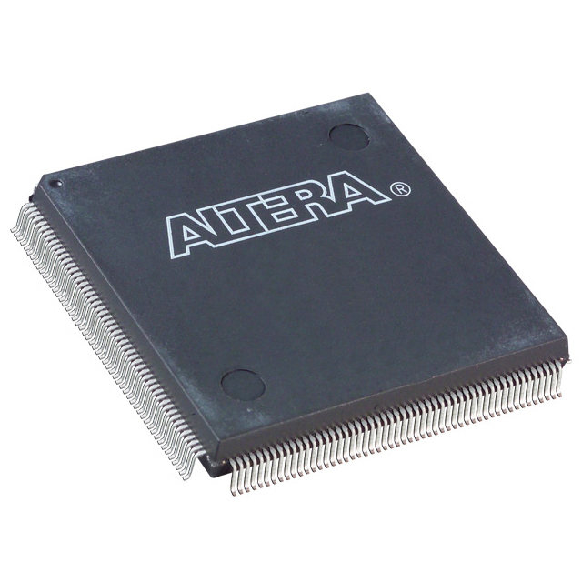
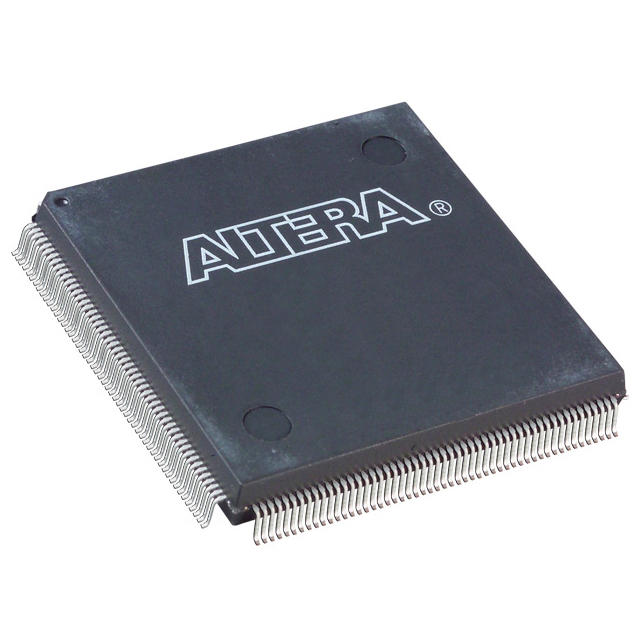
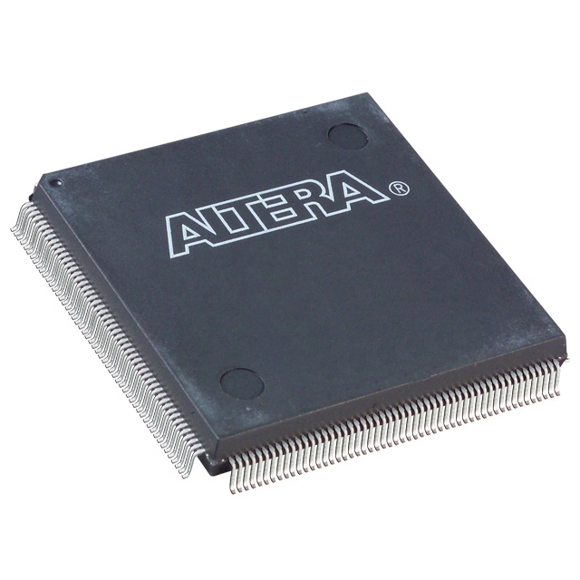
FLEX-10KS® Field Programmable Gate Array (FPGA) IC 147 40960 2880 208-BFQFP |
|---|---|
| Quantity | 1,175 Available (as of October 7, 2026) |
| Product Category | Field Programmable Gate Array (FPGA) |
|---|---|
| Manufacturer | Intel |
| Manufacturing Status | Obsolete |
| Manufacturer Standard Lead Time | Contact Us |
| Datasheet |
Specifications & Environmental
| Device Package | 208-PQFP (28x28) | Grade | Commercial | Operating Temperature | 0°C – 70°C | ||
|---|---|---|---|---|---|---|---|
| Package / Case | 208-BFQFP | Number of I/O | 147 | Voltage | 2.375 V - 2.625 V | ||
| Mounting Method | Surface Mount | RoHS Compliance | Unknown | REACH Compliance | REACH Unaffected | ||
| Moisture Sensitivity Level | 3 (168 Hours) | Number of LABs/CLBs | 360 | Number of Logic Elements/Cells | 2880 | ||
| Number of Gates | 199000 | ECCN | 3A001A2A | HTS Code | 8542.39.0001 | ||
| Qualification | N/A | Total RAM Bits | 40960 |
Overview of EPF10K50SQC208-1X – FLEX-10KS® Field Programmable Gate Array (FPGA) IC 147 40960 2880 208-BFQFP
The EPF10K50SQC208-1X is a FLEX-10KS family field programmable gate array manufactured by Intel, delivering a combination of on-chip memory and reprogrammable logic in a 208‑pin BFQFP package. It integrates 2,880 logic elements across 360 LABs and provides 40,960 bits of embedded RAM alongside 147 user I/O pins, making it suitable for commercial embedded designs that require moderate logic density and significant on-chip memory.
Designed for system-level integration, the device supports in-circuit reconfigurability and family-level features such as embedded arrays for megafunction implementation and dedicated interconnect and arithmetic chains, enabling efficient implementation of memory-intensive and specialized logic functions in surface-mount designs.
Key Features
- Core logic — 2,880 logic elements implemented across 360 LABs, providing a fixed, verifiable logic capacity for medium-complexity FPGA designs.
- Embedded memory — 40,960 total RAM bits of on-chip memory for implementing buffers, FIFOs, and other memory-intensive megafunctions without consuming logic element capacity.
- I/O density — 147 user I/O pins to support a broad range of external interfaces and signal routing in I/O‑heavy applications.
- System-level programmability — In-circuit reconfigurability via external configuration device or JTAG port and built-in JTAG boundary-scan test circuitry for board-level test and reconfiguration.
- Dedicated arithmetic and routing — Family-level features include dedicated carry chains and cascade chains plus the FastTrack interconnect structure for predictable routing and efficient implementation of adders, counters, and high-fan-in logic.
- Package & mounting — Supplied in a 208‑BFQFP (208‑PQFP 28×28) surface-mount package for standard PCB assembly.
- Power and temperature — Voltage supply range 2.375 V to 2.625 V and operating temperature range 0 °C to 70 °C, targeted for commercial-grade applications.
- Compliance — RoHS compliant.
Typical Applications
- System-on-a-programmable-chip (SOPC) integration — Use the device’s embedded arrays and reprogrammable logic to integrate memory and specialized logic functions in compact SOPC designs.
- Memory‑intensive logic — The 40,960 bits of on-chip RAM are well suited for data buffering, FIFOs, and packet-handling functions in communications and embedded systems.
- I/O control and interface bridging — With 147 I/O pins, the device can consolidate multiple peripheral interfaces and handle complex signal routing for custom control panels or protocol converters.
- Prototyping and product development — Reconfigurability and built-in JTAG support enable iterative hardware development, testing, and boundary-scan verification during product bring-up.
Unique Advantages
- Significant on-chip RAM: 40,960 bits of embedded memory reduce external memory requirements and simplify board-level BOM for memory-centric functions.
- Balanced logic and I/O: 2,880 logic elements paired with 147 I/Os provide a practical balance for designs that need both logic capacity and moderate peripheral connectivity.
- Reconfigurable design flow: In-circuit reconfigurability and JTAG boundary-scan support speed up development cycles and enable field updates without board replacement.
- Efficient arithmetic and routing: Dedicated carry and cascade chains plus FastTrack interconnect help implement arithmetic-heavy and high-fan-in logic efficiently.
- Commercial-grade readiness: Surface-mount 208‑BFQFP packaging, defined supply and temperature ranges, and RoHS compliance align the device to commercial embedded product requirements.
Why Choose EPF10K50SQC208-1X?
The EPF10K50SQC208-1X positions itself as a practical, reprogrammable solution where on-chip memory and moderate logic density are priorities. Its combination of 2,880 logic elements, 40,960 bits of embedded RAM, and 147 I/Os supports embedded applications that require memory-intensive megafunctions, interface consolidation, and iterative development through in-circuit reconfiguration and JTAG testing.
This device is suited for commercial embedded designs and development projects that benefit from integrated memory, predictable routing resources, and standard surface-mount packaging. Its family-level features offer engineering teams a clear pathway to implement specialized logic and system-level functions with reduced external components and streamlined board-level testing.
Request a quote or submit an inquiry to receive pricing and availability information for the EPF10K50SQC208-1X and to discuss how this FLEX-10KS device can fit your next embedded design.























Date Founded: 1968
Headquarters: Santa Clara, California, USA
Employees: 130,000+
Revenue: $54.23 Billion
Certifications and Memberships: ISO9001:2015, ISO14001:2015, ISO17025:2017, ISO27001:2022, ISO45001:2018, ISO50001:2018


