
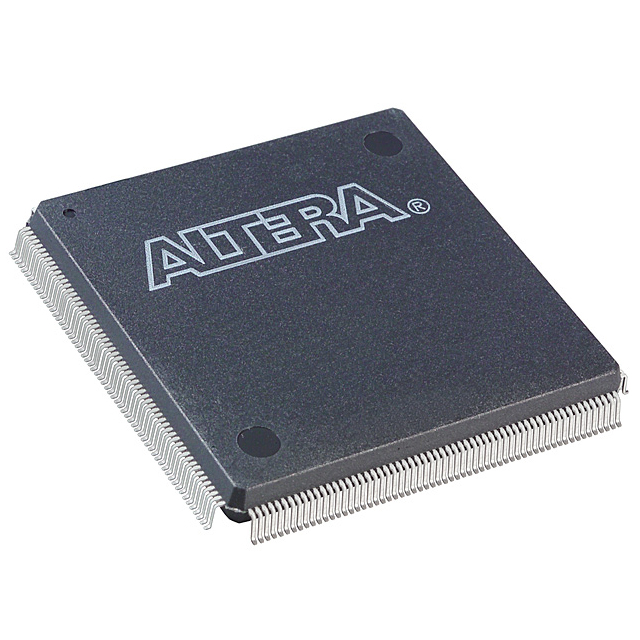
EPF10K50VQC240-3N
| Part Description |
FLEX-10K® Field Programmable Gate Array (FPGA) IC 189 20480 2880 240-BFQFP |
|---|---|
| Quantity | 125 Available (as of June 15, 2026) |
| Product Category | Field Programmable Gate Array (FPGA) |
|---|---|
| Manufacturer | Intel |
| Manufacturing Status | Obsolete |
| Manufacturer Standard Lead Time | Contact Us |
| Datasheet |
Specifications & Environmental
| Device Package | 240-PQFP (32x32) | Grade | Commercial | Operating Temperature | 0°C – 70°C | ||
|---|---|---|---|---|---|---|---|
| Package / Case | 240-BFQFP | Number of I/O | 189 | Voltage | 3 V - 3.6 V | ||
| Mounting Method | Surface Mount | RoHS Compliance | Unknown | REACH Compliance | REACH Unaffected | ||
| Moisture Sensitivity Level | 3 (168 Hours) | Number of LABs/CLBs | 360 | Number of Logic Elements/Cells | 2880 | ||
| Number of Gates | 116000 | ECCN | 3A001A2A | HTS Code | 8542.39.0001 | ||
| Qualification | N/A | Total RAM Bits | 20480 |
Overview of EPF10K50VQC240-3N – FLEX-10K Field Programmable Gate Array (FPGA) IC, 189 I/O, 20,480 RAM bits, 2,880 logic elements, 240-BFQFP
The EPF10K50VQC240-3N is an Intel FLEX-10K series field programmable gate array designed for embedded programmable logic applications. It combines a logic array with embedded memory blocks to implement system-level functions and megafunctions on a single device.
Targeted at commercial designs, this surface-mount device delivers 2,880 logic elements, approximately 20,480 bits of embedded RAM, up to 189 user I/O pins in the 240-BFQFP package, and operates from a 3.0 V to 3.6 V supply across a 0 °C to 70 °C temperature range.
Key Features
- Logic Capacity – 2,880 logic elements and up to 116,000 maximum system gates provide the compute fabric for glue logic, state machines, and custom datapaths.
- Embedded Memory – Approximately 20,480 bits of on-chip RAM implemented via embedded array blocks to support FIFOs, buffers, and small on-chip data storage without consuming logic element capacity.
- I/O and Packaging – 189 user I/O pins in a 240-BFQFP (supplier package: 240-PQFP 32×32) surface-mount package for flexible board-level integration and package-level I/O routing.
- Supply and Commercial Grade – Designed for 3.0 V to 3.6 V operation and specified for commercial temperature operation from 0 °C to 70 °C.
- Reconfiguration and Test – In-circuit reconfigurability via external configuration devices and JTAG boundary-scan support for device programming and board-level testability.
- Clocking and Performance – Built-in low-skew clock distribution trees and options such as ClockLock and ClockBoost to manage clock delay and support high-performance internal timing.
- Fast Interconnect and Arithmetic Support – FastTrack continuous routing structure plus dedicated carry and cascade chains for efficient arithmetic and high-fan-in logic implementations.
- Programmable I/O Controls – Per-pin tri-state output enable, open-drain option, and programmable output slew-rate control to manage interfacing and switching noise.
- Standards & Reliability Features – Built-in IEEE 1149.1 JTAG boundary-scan for board-level test and debug without consuming device logic.
- Compliance – RoHS compliant.
Typical Applications
- Embedded Control – Implement custom control logic, state machines, and peripheral glue in commercial embedded systems using the device’s logic elements and on-chip RAM.
- Interface Bridging – Provide protocol adaptation and bus bridging between subsystems with flexible I/O control and dedicated routing resources.
- Prototyping and Development – Use in hardware prototypes or low- to mid-density programmable designs that require reconfigurability and in-circuit programming via JTAG or external configuration devices.
- Data Buffering and Small Memories – Take advantage of embedded RAM blocks for FIFOs, packet buffers, and temporary storage without consuming additional logic cells.
Unique Advantages
- Balanced Logic and Memory: The combination of 2,880 logic elements and approximately 20,480 bits of embedded RAM lets you implement control, combinational logic, and local data storage within the same device.
- Flexible I/O in a Compact Package: 189 user I/Os in a 240-pin BFQFP package provide a dense I/O count for board designs that require many external interfaces while remaining surface-mount friendly.
- Reconfigurability and Testability: In-circuit reconfiguration and IEEE 1149.1 JTAG boundary-scan support simplify firmware updates and board-level diagnostics.
- Deterministic Routing and Arithmetic Support: FastTrack routing and dedicated carry/cascade chains reduce routing uncertainty and accelerate arithmetic implementations.
- Programmable I/O Behavior: Per-pin tri-state enable, open-drain option, and slew-rate control allow precise signal integrity and interfacing adjustments without additional components.
- Standards-Conscious Design: RoHS compliance and commercial-grade specifications align the device with common electronics manufacturing and environmental requirements.
Why Choose EPF10K50VQC240-3N?
The EPF10K50VQC240-3N provides a well-rounded programmable logic option for commercial embedded designs that need a mix of logic resources, on-chip RAM, and flexible I/O in a 240-pin surface-mount package. Its built-in reconfiguration, JTAG support, deterministic interconnect, and dedicated arithmetic resources make it suitable for applications requiring in-field updates, prototyping, or medium-complexity system glue logic.
This part is appropriate for teams seeking a commercially graded FPGA solution with explicit on-chip memory, a clear voltage and temperature specification, and features that simplify board-level integration and test.
Request a quote or submit a procurement inquiry to obtain pricing, lead time, and availability for the EPF10K50VQC240-3N. Include your required quantities and target delivery timeframe for a tailored response.


Date Founded: 1968
Headquarters: Santa Clara, California, USA
Employees: 130,000+
Revenue: $54.23 Billion
Certifications and Memberships: ISO9001:2015, ISO14001:2015, ISO17025:2017, ISO27001:2022, ISO45001:2018, ISO50001:2018


