
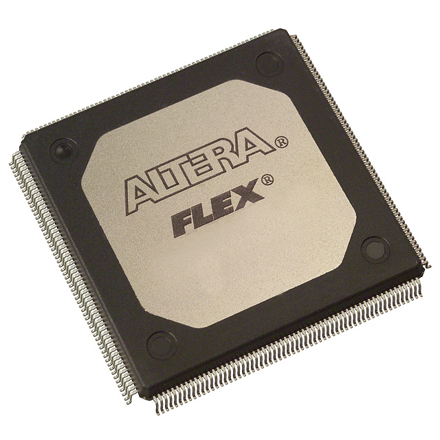
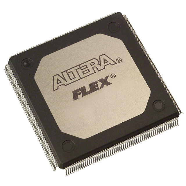
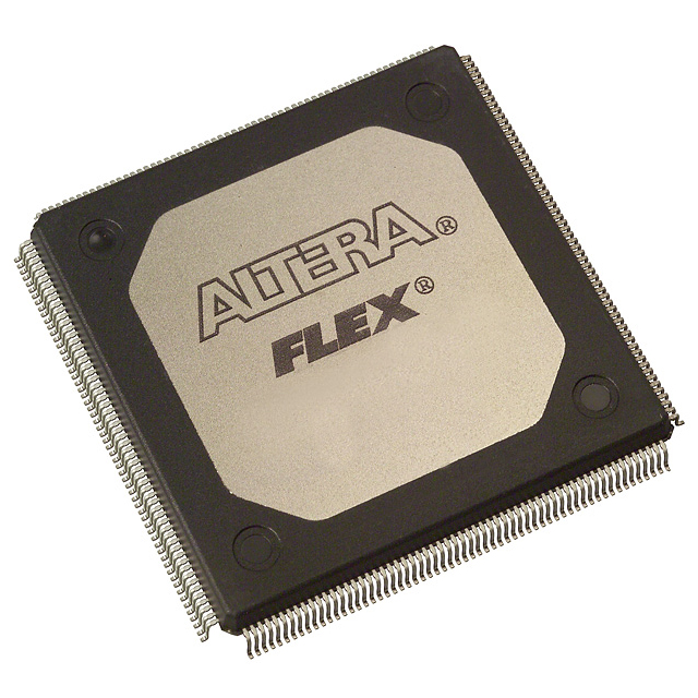
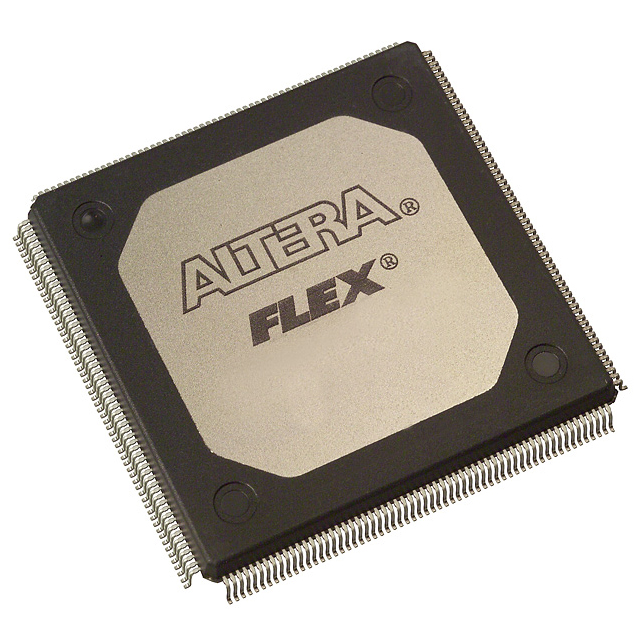
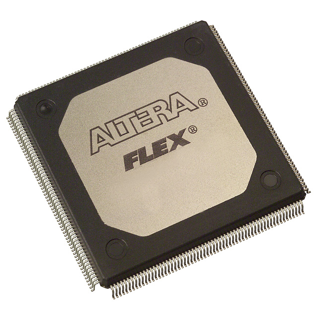
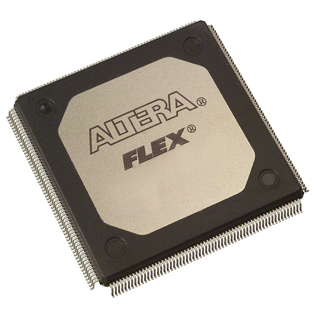
EPF10K50VRC240-3
| Part Description |
FLEX-10K® Field Programmable Gate Array (FPGA) IC 189 20480 2880 240-BFQFP Exposed Pad |
|---|---|
| Quantity | 1,739 Available (as of October 8, 2026) |
| Product Category | Field Programmable Gate Array (FPGA) |
|---|---|
| Manufacturer | Intel |
| Manufacturing Status | Obsolete |
| Manufacturer Standard Lead Time | Contact Us |
| Datasheet |
Specifications & Environmental
| Device Package | 240-RQFP (32x32) | Grade | Commercial | Operating Temperature | 0°C – 70°C | ||
|---|---|---|---|---|---|---|---|
| Package / Case | 240-BFQFP Exposed Pad | Number of I/O | 189 | Voltage | 3 V - 3.6 V | ||
| Mounting Method | Surface Mount | RoHS Compliance | RoHS non-compliant | REACH Compliance | REACH Unaffected | ||
| Moisture Sensitivity Level | 3 (168 Hours) | Number of LABs/CLBs | 360 | Number of Logic Elements/Cells | 2880 | ||
| Number of Gates | 116000 | ECCN | 3A991D | HTS Code | 8542.39.0001 | ||
| Qualification | N/A | Total RAM Bits | 20480 |
Overview of EPF10K50VRC240-3 – FLEX-10K FPGA, 2,880 logic elements, 20,480-bit RAM, 189 I/O, 240-BFQFP
The EPF10K50VRC240-3 is a commercial-grade FLEX-10K field-programmable device from Intel (Altera) that combines a logic array and embedded memory to support System-on-a-Programmable-Chip (SOPC) integration. Built on the FLEX 10K family architecture, it provides embedded array blocks for efficient on-chip memory and megafunction implementation alongside a flexible logic fabric.
With 2,880 logic elements, 20,480 bits of embedded RAM, and 189 user I/Os in a 240-pin exposed-pad surface-mount package, this device targets designs that require mid-range logic density, substantial on-chip memory, and flexible I/O for commercial embedded applications.
Key Features
- Logic and Array Resources 2,880 logic elements (LEs) and 360 logic array blocks (LABs), supporting up to 116,000 maximum system gates for mid-density logic implementations.
- Embedded Memory Ten embedded array blocks (EABs) totaling 20,480 bits of on-chip RAM to implement efficient memory and specialized logic megafunctions without reducing logic capacity.
- I/O and Package 189 user I/O pins in a 240-BFQFP exposed-pad package (supplier device package: 240-RQFP, 32×32); surface-mount mounting for standard board assembly.
- Supply and Temperature Operates from 3.0 V to 3.6 V and is rated for commercial operating temperatures from 0 °C to 70 °C.
- Configuration and Test In-circuit reconfigurability via external configuration devices, intelligent controllers, or the JTAG port. Built-in IEEE 1149.1 JTAG boundary-scan test circuitry is available without consuming device logic.
- Interconnect and Arithmetic Support FastTrack continuous routing, dedicated carry chains for fast arithmetic, and dedicated cascade chains for high-fan-in logic accelerate implementation of adders, counters, and complex combinational functions.
- Clocking and Control Built-in low-skew clock distribution trees, support for up to six global clock signals and four global clear signals, and options for ClockLock and ClockBoost to control clock delay and multiplication at the family level.
- Pin-level Flexibility Individual tri-state output enable per pin, open-drain option on each I/O pin, and programmable output slew-rate control to help manage signal integrity and interfacing.
- RoHS Compliant Meets RoHS environmental requirements for lead-free assembly.
Typical Applications
- System-on-a-Programmable-Chip (SOPC) integration Implement embedded memory, custom peripherals, and specialized logic blocks on a single programmable device to reduce board-level component count.
- Memory-intensive logic functions Use the ten EABs and 20,480 bits of on-chip RAM for buffering, lookup tables, and megafunctions that require on-chip storage.
- Interface bridging and I/O aggregation Leverage 189 user I/Os to implement protocol converters, bus bridges, and mid-density I/O aggregation in commercial embedded products.
- Prototype and product-level custom logic Ideal for commercial embedded designs needing reconfigurability, boundary-scan test support, and mid-range gate density for custom logic implementations.
Unique Advantages
- Highly integrated mid-density logic Combines 2,880 LEs with substantial embedded RAM to implement compact, multi-function designs on a single device.
- Dedicated hardware for arithmetic and high-fan-in logic Built-in carry and cascade chains reduce routing and logic resource usage for adders, counters, and complex combinational functions.
- Robust configuration and testability In-circuit reconfigurability and IEEE 1149.1 JTAG boundary-scan provide flexible programming and board-level test options without consuming user logic.
- Flexible clocking and low-skew distribution Multiple global clocks and low-skew clock trees simplify synchronous design and timing distribution for multi-clock systems.
- Commercial-grade packaging and compliance Surface-mount 240-BFQFP exposed-pad package for standard assembly flows and RoHS compliance for lead-free manufacturing.
- Design tool support The FLEX 10K family includes software design and automatic place-and-route support from Altera development systems for common workstation environments, easing implementation and bring-up.
Why Choose EPF10K50VRC240-3?
The EPF10K50VRC240-3 delivers a balanced combination of logic density, on-chip memory, and I/O capacity in a commercial-grade FLEX 10K device. Its embedded array blocks, dedicated arithmetic/cascade resources, and comprehensive configuration and test capabilities make it well suited for mid-range embedded applications that require reconfigurability and on-chip memory without sacrificing board-level simplicity.
Choose this device for designs that need scalable logic and memory resources, flexible I/O, and proven family-level features such as JTAG boundary-scan and software design support—providing a platform that simplifies integration and shortens development cycles for commercial embedded products.
Request a quote or submit a product inquiry to receive pricing and availability details for the EPF10K50VRC240-3.





















Date Founded: 1968
Headquarters: Santa Clara, California, USA
Employees: 130,000+
Revenue: $54.23 Billion
Certifications and Memberships: ISO9001:2015, ISO14001:2015, ISO17025:2017, ISO27001:2022, ISO45001:2018, ISO50001:2018


