
EPF10K50VRC240-4
| Part Description |
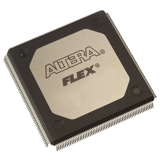
FLEX-10K® Field Programmable Gate Array (FPGA) IC 189 20480 2880 240-BFQFP Exposed Pad |
|---|---|
| Quantity | 524 Available (as of June 14, 2026) |

| Product Category | Field Programmable Gate Array (FPGA) |
|---|---|
| Manufacturer | Intel |
| Manufacturing Status | Obsolete |
| Manufacturer Standard Lead Time | Contact Us |
| Datasheet |
Specifications & Environmental
| Device Package | 240-RQFP (32x32) | Grade | Commercial | Operating Temperature | 0°C – 70°C | ||
|---|---|---|---|---|---|---|---|
| Package / Case | 240-BFQFP Exposed Pad | Number of I/O | 189 | Voltage | 3 V - 3.6 V | ||
| Mounting Method | Surface Mount | RoHS Compliance | RoHS non-compliant | REACH Compliance | REACH Unaffected | ||
| Moisture Sensitivity Level | 3 (168 Hours) | Number of LABs/CLBs | 360 | Number of Logic Elements/Cells | 2880 | ||
| Number of Gates | 116000 | ECCN | 3A991D | HTS Code | 8542.39.0001 | ||
| Qualification | N/A | Total RAM Bits | 20480 |
Overview of EPF10K50VRC240-4 – FLEX-10K® Field Programmable Gate Array (FPGA), 189 I/O, 20,480-bit RAM
The EPF10K50VRC240-4 is a FLEX-10K family FPGA offering a mid-range logic and embedded-memory solution for commercial applications. It combines a dedicated logic array and embedded array blocks for implementing general logic and megafunctions, enabling System-on-a-Programmable-Chip (SOPC) integration and efficient on-chip memory usage.
Designed for surface-mount applications, this device provides 2,880 logic elements (LEs), approximately 20,480 bits of embedded RAM, up to 189 user I/Os, and a 240-pin BFQFP exposed-pad package. The device operates from 3.0 V to 3.6 V with a commercial temperature range of 0 °C to 70 °C and is RoHS compliant.
Key Features
- Core Logic 2,880 logic elements and 360 LABs provide the programmable fabric for implementing combinational and sequential logic functions.
- Embedded Memory Approximately 20,480 bits of embedded RAM distributed across embedded array blocks (EABs) to support megafunctions and on-chip data storage.
- Capacity (Gates) Device-level capacity reported as 116,000 maximum system gates for integrating substantial logic and memory resources on a single IC.
- I/O and Interfaces Up to 189 user I/O pins with per-pin control options for flexible interfacing in multi-voltage systems.
- Configuration & Test In-circuit reconfigurability via external configuration device or JTAG; built-in JTAG boundary-scan circuitry for board-level testability.
- Clocking & Interconnect Family features include low-skew clock distribution, dedicated carry and cascade chains, and a continuous routing structure to support predictable interconnect delays and arithmetic functions.
- Power & Supply Voltage supply range of 3.0 V to 3.6 V supports 3.3 V system designs; surface-mount mounting type and exposed-pad BFQFP package aid thermal management and board assembly.
- Package & Mechanical 240-BFQFP exposed pad (supplier package: 240-RQFP, 32×32) for surface-mount placement and integration into space-constrained boards.
- Compliance & Grade Commercial grade device (0 °C to 70 °C) and RoHS compliant.
Typical Applications
- System Integration / SOPC Use the device's embedded arrays and logic fabric to consolidate memory and specialized logic into a System-on-a-Programmable-Chip architecture.
- Interface Bridging and I/O Expansion Leverage up to 189 I/Os to implement protocol bridging, level translation, or custom peripheral interfaces on a single FPGA.
- Embedded Control and Glue Logic Implement control state machines, peripheral controllers, and glue logic using the device's logic elements and embedded RAM.
- Megafunction Implementation Deploy efficient memory-based megafunctions and specialized logic using the device's EABs and dedicated arithmetic/cascade chains.
Unique Advantages
- Integrated Memory and Logic: Approximately 20,480 bits of embedded RAM combined with 2,880 logic elements reduces external memory needs and simplifies board design.
- Substantial I/O Count: Up to 189 user I/Os enable dense peripheral connectivity and flexible interface options without additional I/O expanders.
- In-Circuit Reconfigurability: Supports reconfiguration via external devices or JTAG, enabling field-updatable logic and late-stage design changes.
- Dedicated Arithmetic Resources: Carry and cascade chains accelerate implementation of adders, counters, and high-fan-in logic, improving performance for arithmetic- and control-heavy designs.
- Package for Thermal Management: 240-BFQFP exposed-pad package supports heat dissipation and reliable surface-mount assembly in commercial electronics.
- Testability: Built-in JTAG boundary-scan facilitates board-level test and debug without consuming device logic.
Why Choose EPF10K50VRC240-4?
The EPF10K50VRC240-4 positions itself as a versatile mid-range FPGA for designers who need a balanced combination of logic capacity, embedded memory, and I/O density in a commercial-grade device. Its flexible fabric and embedded array architecture support SOPC integration and efficient implementation of megafunctions while providing built-in test and reconfiguration capabilities.
This device is well suited for applications requiring significant on-chip RAM, multiple dedicated arithmetic resources, and a high number of I/Os within a 240-pin BFQFP exposed-pad surface-mount package. The combination of programmable resources and configuration options supports iterative development and long-term design scalability within the FLEX-10K family.
Request a quote or submit an RFQ to evaluate EPF10K50VRC240-4 for your next design project.


Date Founded: 1968
Headquarters: Santa Clara, California, USA
Employees: 130,000+
Revenue: $54.23 Billion
Certifications and Memberships: ISO9001:2015, ISO14001:2015, ISO17025:2017, ISO27001:2022, ISO45001:2018, ISO50001:2018


