
HC20K1000FC672
| Part Description |
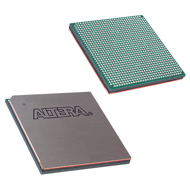
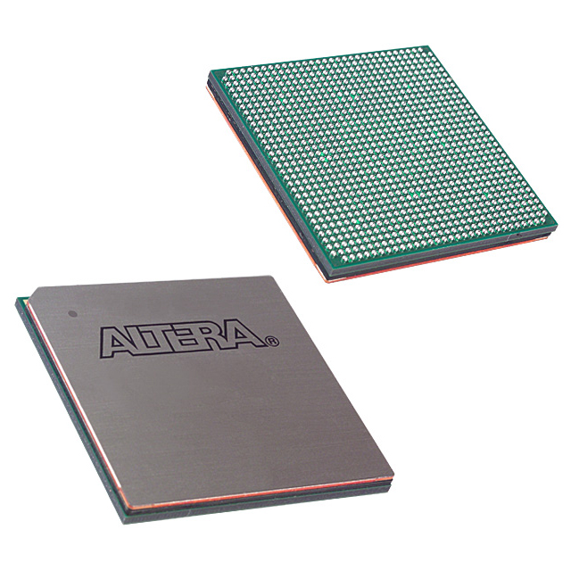
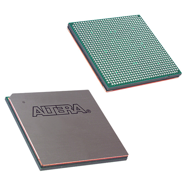
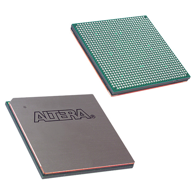
APEX® HardCopy® Field Programmable Gate Array (FPGA) IC 327680 38400 672-BBGA |
|---|---|
| Quantity | 80 Available (as of October 8, 2026) |

| Product Category | Field Programmable Gate Array (FPGA) |
|---|---|
| Manufacturer | Intel |
| Manufacturing Status | Obsolete |
| Manufacturer Standard Lead Time | Contact Us |
| Datasheet |
Specifications & Environmental
| Device Package | 672-FBGA (27x27) | Grade | Commercial | Operating Temperature | 0°C – 85°C | ||
|---|---|---|---|---|---|---|---|
| Package / Case | 672-BBGA | Number of I/O | 488 | Voltage | 1.71 V - 1.89 V | ||
| Mounting Method | Surface Mount | RoHS Compliance | RoHS non-compliant | REACH Compliance | REACH Unknown | ||
| Moisture Sensitivity Level | 3 (168 Hours) | Number of LABs/CLBs | N/A | Number of Logic Elements/Cells | 38400 | ||
| Number of Gates | 1000000 | ECCN | OBSOLETE | HTS Code | 0000.00.0000 | ||
| Qualification | N/A | Total RAM Bits | 327680 |
Overview of HC20K1000FC672 – APEX® HardCopy® Field Programmable Gate Array (FPGA) IC 327680 38400 672-BBGA
The HC20K1000FC672 is a commercial-grade APEX® HardCopy® device that brings APEX 20KE technology into high-volume, cost-sensitive production. It implements a high-density multiCore architecture with embedded memory and look-up table logic aimed at register‑intensive and memory‑centric functions.
Designed for surface-mount deployment in a 672‑BBGA (supplier package: 672‑FBGA, 27×27), this RoHS‑compliant device provides 38,400 logic elements, 327,680 bits of embedded RAM and a broad I/O complement for systems requiring significant logic integration and flexible I/O support while operating within a 1.71 V to 1.89 V core supply range and 0 °C to 85 °C commercial temperature window.
Key Features
- Core density and gates — 38,400 logic elements and 1,000,000 gates deliver substantial programmable logic capacity for complex system functions.
- Embedded memory — 327,680 total RAM bits (approximately 0.33 Mbits) with Embedded System Blocks (ESBs) for FIFO, dual-port RAM and CAM implementations.
- I/O and interfacing — 488 user I/O pins in the 672‑BBGA package with MultiVolt I/O support for 1.8 V, 2.5 V and 3.3 V interfaces and dedicated LVDS channels described for series devices.
- Clock management — Series-level clock resources include up to four phase-locked loops (PLLs), a built-in low‑skew clock tree and multiple global clock signals for complex timing domains.
- Process and customization — Manufactured on a 0.18‑µm CMOS, six‑layer‑metal process; device customization is performed through metallization layers as part of the HardCopy flow.
- Power and voltage — Low-power device architecture with a specified core voltage supply range of 1.71 V to 1.89 V and series features supporting power-saving ESB modes.
- Packaging and mounting — Surface mount 672‑BBGA package (supplier: 672‑FBGA, 27×27) for dense board-level integration.
- Commercial reliability — Commercial grade operation across 0 °C to 85 °C with RoHS compliance.
Typical Applications
- High‑volume consumer and communications products — Integrate complex control, protocol handling, and glue‑logic into a single device to reduce BOM and streamline production.
- Memory interface and buffering — Use embedded RAM and ESBs to implement FIFOs, dual‑port RAM and CAM functions for data buffering and packet processing.
- Clocked digital systems — Leverage multi‑PLL and low‑skew clocking for multi‑domain timing control in systems with demanding synchronization requirements.
- High‑density logic consolidation — Consolidate multiple discrete logic functions into one 38,400‑LE device to simplify board design and lower part counts.
Unique Advantages
- High-density programmable fabric: 38,400 logic elements and 1,000,000 gates provide the capacity to integrate complex logic functions without multiple devices.
- Built-in memory resources: 327,680 bits of embedded RAM and ESBs reduce external memory requirements for buffering and state storage.
- Flexible I/O support: 488 user I/Os and MultiVolt I/O capability enable direct interfacing to a wide range of peripherals and bus standards at the board level.
- Robust clocking options: Up to four PLLs and a low‑skew clock tree support multiple synchronous domains and precise timing control.
- Production-ready packaging: 672‑BBGA surface-mount package (672‑FBGA, 27×27) facilitates automated assembly in high-volume manufacturing.
- Compliance and assembly readiness: RoHS‑compliant construction and commercial temperature grading simplify procurement and integration for mainstream products.
Why Choose HC20K1000FC672?
The HC20K1000FC672 positions APEX HardCopy density and embedded system resources in a production-friendly, surface‑mount package. It is well suited for designers moving from prototype programmable logic to a HardCopy device that preserves architecture and timing while enabling cost‑effective volume production.
This device is appropriate for teams seeking to consolidate logic, accelerate time to market, and leverage embedded memory and advanced clocking in commercial‑temperature applications. Its multiCore architecture, ESBs, and flexible I/O support offer a clear path to reduce external components and simplify board design while meeting standard manufacturing requirements.
Request a quote or submit a product inquiry to receive pricing and availability information for HC20K1000FC672 and to discuss fitment in your next production design.






















Date Founded: 1968
Headquarters: Santa Clara, California, USA
Employees: 130,000+
Revenue: $54.23 Billion
Certifications and Memberships: ISO9001:2015, ISO14001:2015, ISO17025:2017, ISO27001:2022, ISO45001:2018, ISO50001:2018


