
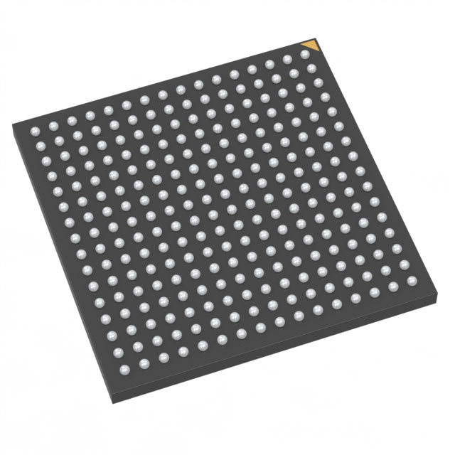
M1A3P1000-1FG144M
| Part Description |
ProASIC3 Field Programmable Gate Array (FPGA) IC 97 147456 144-LBGA |
|---|---|
| Quantity | 844 Available (as of June 14, 2026) |

| Product Category | Field Programmable Gate Array (FPGA) |
|---|---|
| Manufacturer | Microchip Technology |
| Manufacturing Status | Active |
| Manufacturer Standard Lead Time | 24 Weeks |
| Datasheet |
Specifications & Environmental
| Device Package | 144-FPBGA (13x13) | Grade | Military | Operating Temperature | -55°C – 125°C | ||
|---|---|---|---|---|---|---|---|
| Package / Case | 144-LBGA | Number of I/O | 97 | Voltage | 1.425 V - 1.575 V | ||
| Mounting Method | Surface Mount | RoHS Compliance | RoHS non-compliant | REACH Compliance | REACH Unaffected | ||
| Moisture Sensitivity Level | 3 (168 Hours) | Number of LABs/CLBs | 24576 | Number of Logic Elements/Cells | 24576 | ||
| Number of Gates | 1000000 | ECCN | 3A001A2C | HTS Code | 8542.39.0001 | ||
| Qualification | MIL-STD-883 | Total RAM Bits | 147456 |
Overview of M1A3P1000-1FG144M – ProASIC3 FPGA, 97 I/O, 144-LBGA
The M1A3P1000-1FG144M is a ProASIC3 Field Programmable Gate Array (FPGA) IC from Microchip Technology designed for military-grade embedded applications. It provides a high density of programmable logic and on-chip memory combined with a 97-pin I/O interface and a compact 144-LBGA package.
With 24,576 logic elements, approximately 0.147 Mbits of embedded memory, and a 1,000,000-gate capacity, this device targets systems that require significant integration and reliability across a wide operating temperature range and MIL-STD-883 qualification.
Key Features
- Core Logic 24,576 logic elements (cells) and a gate count of 1,000,000 provide substantial programmable logic capacity for complex digital designs.
- Embedded Memory 147,456 bits of on-chip RAM — approximately 0.147 Mbits — to support buffering, state storage, and small-data processing tasks without external memory.
- I/O Resources 97 user I/O pins for interfacing to peripherals, sensors, and external modules in dense system designs.
- Power Single-supply operation with a supply voltage range of 1.425 V to 1.575 V to match targeted system power rails.
- Package and Mounting 144-LBGA package (supplier device package: 144-FPBGA 13×13) in a surface-mount form factor for compact board-level integration.
- Military-Grade Qualification Military grade device qualified to MIL-STD-883 and rated for operation from −55 °C to 125 °C for use in harsh environments.
Typical Applications
- Military & Defense Systems — Suitable for tactical electronics and ruggedized subsystems that require MIL-STD-883 qualification and wide temperature operation.
- Aerospace Avionics — Use in avionics control, signal processing, and interface conversion where high logic density and military-grade qualification are required.
- Industrial Control — Implementation of motor control, process automation logic, and safety monitoring in high-temperature or demanding industrial environments.
- Communications & Networking — Protocol bridging, packet-processing logic, and custom interface implementations leveraging the device’s logic density and I/O resources.
- Instrumentation & Test Equipment — On-board data handling, timing logic, and control functions for measurement systems that require robust operation across temperature extremes.
Unique Advantages
- Military-qualified robustness: MIL-STD-883 qualification plus an operating range of −55 °C to 125 °C supports deployment in demanding environments.
- High integration density: 24,576 logic elements and 1,000,000 gates reduce the need for multiple discrete components and help shrink BOM size.
- On-chip memory availability: Approximately 0.147 Mbits of embedded RAM enables local buffering and state storage without immediate reliance on external memory devices.
- Versatile I/O count: 97 I/O pins provide flexible interfacing for mixed-signal front-ends, sensors, and external controllers.
- Compact, surface-mount package: 144-LBGA (144-FPBGA 13×13) simplifies PCB layout for space-constrained systems while supporting standard assembly processes.
- Narrow supply range: Defined supply voltage window (1.425 V to 1.575 V) helps ensure predictable power design and integration with system rails.
Why Choose M1A3P1000-1FG144M?
The M1A3P1000-1FG144M positions itself as a military-grade FPGA option for designs that require a balance of logic capacity, on-chip memory, and rugged qualification. Its combination of 24,576 logic elements, roughly 0.147 Mbits of embedded RAM, and a 97-pin I/O arrangement offers designers a well-specified platform for dense, reliable digital implementations.
This device is well suited to engineers developing defense, aerospace, industrial, communications, and instrumentation systems where qualification, temperature resilience, and integration density contribute to long-term value and system robustness.
Request a quote or submit a pricing inquiry for the M1A3P1000-1FG144M to evaluate availability and lead times for your next design.


Date Founded: 1989
Headquarters: Chandler, Arizona, USA
Employees: 22,000+
Revenue: $8.349 Billion
Certifications and Memberships: ISO9001:2015, IATF16949:2016, AS 9100D


