
M1A3P1000-1FG256
| Part Description |
ProASIC3 Field Programmable Gate Array (FPGA) IC 177 147456 256-LBGA |
|---|---|
| Quantity | 1,876 Available (as of June 14, 2026) |

| Product Category | Field Programmable Gate Array (FPGA) |
|---|---|
| Manufacturer | Microchip Technology |
| Manufacturing Status | Active |
| Manufacturer Standard Lead Time | 18 Weeks |
| Datasheet |
Specifications & Environmental
| Device Package | 256-FPBGA (17x17) | Grade | Commercial | Operating Temperature | 0°C – 85°C | ||
|---|---|---|---|---|---|---|---|
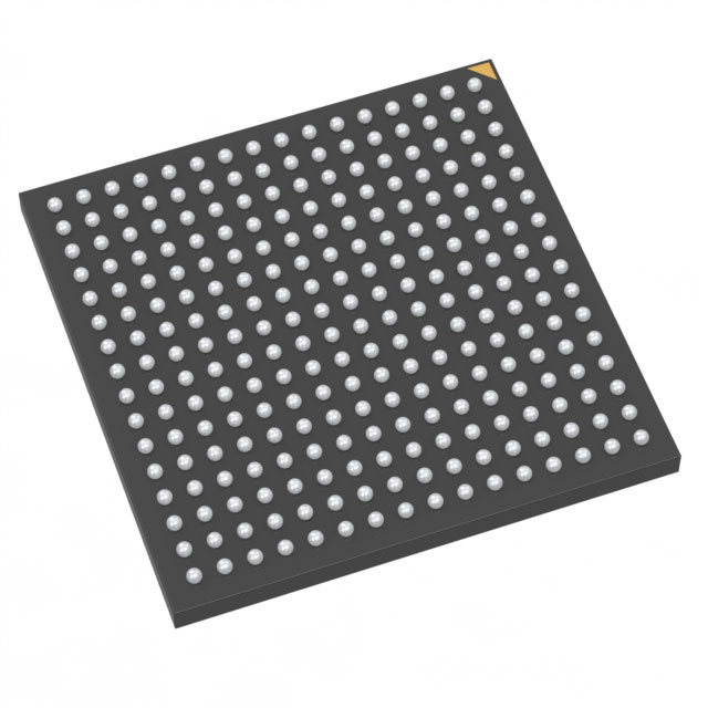
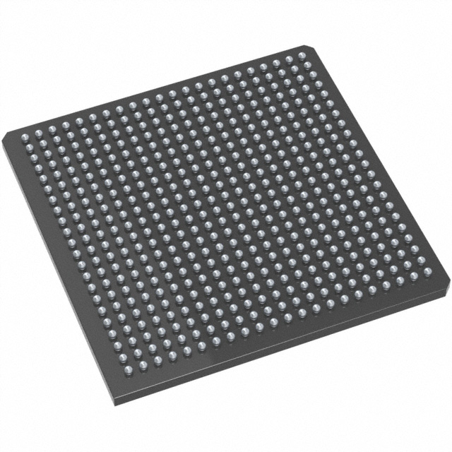
| Package / Case | 256-LBGA | Number of I/O | 177 | Voltage | 1.425 V - 1.575 V | ||
| Mounting Method | Surface Mount | RoHS Compliance | RoHS non-compliant | REACH Compliance | REACH Unaffected | ||
| Moisture Sensitivity Level | 3 (168 Hours) | Number of LABs/CLBs | 24576 | Number of Logic Elements/Cells | 24576 | ||
| Number of Gates | 1000000 | ECCN | 3A991D | HTS Code | 8542.39.0001 | ||
| Qualification | N/A | Total RAM Bits | 147456 |
Overview of M1A3P1000-1FG256 – ProASIC3 Flash FPGA, 1,000,000 Gates, 177 I/O, 256-LBGA
The M1A3P1000-1FG256 is a ProASIC3 field programmable gate array (FPGA) from Microchip Technology. It delivers up to 1,000,000 gates implemented across 24,576 logic elements and provides 177 user I/O signals in a compact 256-LBGA package.
Designed for commercial embedded systems, this low-power flash-based FPGA targets designs that require a balance of logic density, moderate embedded memory, and flexible I/O in a space-efficient package. The device operates from a core supply range of 1.425 V to 1.575 V and supports an operating temperature range of 0 °C to 85 °C.
Key Features
- Core Performance — Up to 1,000,000 gates implemented across 24,576 logic elements to support complex custom digital logic and glue-logic integration.
- Embedded Memory — Approximately 0.147 Mbits (147,456 bits) of on-chip RAM for small to moderate buffering, state machines, and table storage.
- I/O Capacity — 177 user I/O pins to support multiple parallel interfaces, buses, and peripheral connections.
- Flash-Based Architecture — Series-level Flash*Freeze technology referenced in the ProASIC3 family documentation for flash-based configuration and low-power operation.
- Power and Voltage — Core voltage supply range of 1.425 V to 1.575 V for precise power provisioning in embedded designs.
- Package — 256-LBGA (supplier device package: 256-FPBGA, 17×17) providing a compact, high-density footprint for board-level integration.
- Operating Temperature — Commercial temperature grade with an operating range of 0 °C to 85 °C suitable for standard commercial environments.
- Mounting Type — Surface mount package format for standard PCB assembly processes.
Typical Applications
- Embedded Control and Glue Logic — Use where up to 1,000,000 gates and 24,576 logic elements are needed to implement customized control, protocol bridging, or interface logic.
- Multi‑I/O Interface Designs — Ideal for systems requiring many parallel I/Os (177 pins) for sensor arrays, peripheral aggregation, or multi-channel data routing.
- Low‑Power Commercial Systems — Suitable for commercial embedded products that benefit from flash-based configuration and the ProASIC3 family’s low-power characteristics.
Unique Advantages
- High Logic Density: 1,000,000 gates and 24,576 logic elements enable consolidation of multiple discrete functions into a single programmable device, reducing BOM complexity.
- Generous I/O Count: 177 user I/Os provide flexibility for multiple simultaneous interfaces without external multiplexing.
- On‑Chip Memory: Approximately 0.147 Mbits of embedded RAM supports localized buffering and state storage, simplifying board-level memory requirements.
- Compact Packaging: 256-LBGA (256-FPBGA, 17×17) minimizes PCB area while maintaining high signal density for space-constrained designs.
- Controlled Core Supply: Narrow core voltage range (1.425 V–1.575 V) assists in predictable power budgeting and stable device operation.
- Commercial‑Grade Thermal Range: Rated for 0 °C to 85 °C, suitable for standard commercial deployments and typical indoor operating conditions.
Why Choose M1A3P1000-1FG256?
The M1A3P1000-1FG256 positions itself as a compact, flash-configured FPGA option for commercial embedded designs that require substantial programmable logic, a high I/O count, and on-chip RAM in a space-efficient BGA package. Its specifications make it well-suited to engineers consolidating logic functions, implementing multi‑channel interfaces, or optimizing board-level integration.
Backed by the ProASIC3 family documentation from Microchip Technology, this device is a practical choice for projects where predictable core voltage, commercial temperature operation, and a flash-based configuration architecture are important selection criteria.
Request a quote or submit an inquiry to obtain pricing, lead-time, and availability for the M1A3P1000-1FG256.


Date Founded: 1989
Headquarters: Chandler, Arizona, USA
Employees: 22,000+
Revenue: $8.349 Billion
Certifications and Memberships: ISO9001:2015, IATF16949:2016, AS 9100D


