
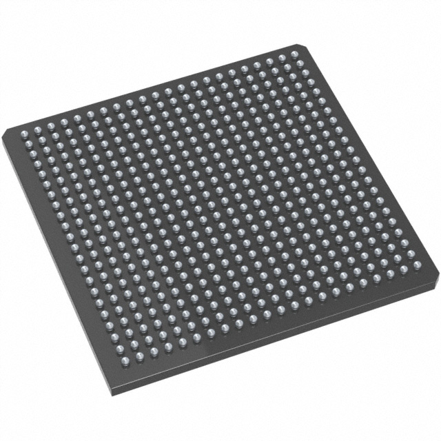
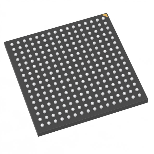
M1AFS1500-2FG676
| Part Description |
Fusion® Field Programmable Gate Array (FPGA) IC 252 276480 676-BGA |
|---|---|
| Quantity | 1 Available (as of June 18, 2026) |

| Product Category | Field Programmable Gate Array (FPGA) |
|---|---|
| Manufacturer | Microchip Technology |
| Manufacturing Status | Active |
| Manufacturer Standard Lead Time | 52 Weeks |
| Datasheet |
Specifications & Environmental
| Device Package | 676-FBGA (27x27) | Grade | Commercial | Operating Temperature | 0°C – 85°C | ||
|---|---|---|---|---|---|---|---|
| Package / Case | 676-BGA | Number of I/O | 252 | Voltage | 1.425 V - 1.575 V | ||
| Mounting Method | Surface Mount | RoHS Compliance | RoHS non-compliant | REACH Compliance | REACH Unaffected | ||
| Moisture Sensitivity Level | 3 (168 Hours) | Number of LABs/CLBs | 38400 | Number of Logic Elements/Cells | 38400 | ||
| Number of Gates | 1500000 | ECCN | 3A991D | HTS Code | 8542.39.0001 | ||
| Qualification | N/A | Total RAM Bits | 276480 |
Overview of M1AFS1500-2FG676 – Fusion® Field Programmable Gate Array (FPGA) IC, 252 I/O, 676-BGA
The M1AFS1500-2FG676 is a Fusion® Field Programmable Gate Array (FPGA) from Microchip Technology designed for programmable-logic implementations requiring high logic density and a large I/O count. It integrates a substantial complement of logic elements, embedded RAM and I/O in a compact 676-ball FBGA package to address space-constrained commercial designs.
Key Features
- Logic Capacity Provides 38,400 logic elements (cells) and approximately 1,500,000 gates to implement complex digital functions and custom logic architectures.
- Embedded Memory Includes approximately 0.28 Mbits (276,480 bits) of total on-chip RAM for buffers, FIFOs and small data structures required by embedded logic.
- I/O Resources Offers 252 user I/O pins to support multiple interfaces, parallel buses and high-pin-count connectivity requirements.
- Package Supplied in a 676-ball FBGA (27 × 27 mm) package for high-density mounting and compact board-level integration.
- Power Operates from a core supply range of 1.425 V to 1.575 V, enabling predictable power sequencing and supply planning.
- Operating Range & Grade Commercial-grade device specified for 0 °C to 85 °C operation and surface-mount assembly.
- Regulatory RoHS compliant for lead-free design and manufacturing requirements.
Typical Applications
- High-Density Control Logic Use the device to implement complex control, sequencing and custom processing functions that require large logic capacity and on-chip RAM.
- I/O-Intensive Interfaces Ideal for designs that need numerous general-purpose I/Os or multiple parallel interfaces, leveraging the 252 available I/O pins.
- Compact Embedded Systems Fits space-constrained assemblies that benefit from a high-pin-count FPGA in a 676-FBGA (27 × 27 mm) package.
- Commercial Electronics Targets commercial-temperature applications where a combination of logic density and integration simplifies system design.
Unique Advantages
- High logic integration: 38,400 logic elements and 1.5 million gates enable implementation of sizable custom digital subsystems on a single device.
- On-chip memory for buffering: 276,480 bits of embedded RAM reduce external memory dependencies for small to moderate buffering needs.
- Extensive I/O capability: 252 user I/Os support multiple interfaces and parallel connections without immediate need for external I/O expanders.
- Compact, manufacturable package: 676-FBGA (27 × 27 mm) provides a small footprint for high-density PCB layouts while supporting surface-mount assembly.
- Commercial-temperature suitability: Specified for 0 °C to 85 °C operation to meet common commercial electronics deployment requirements.
- RoHS compliant: Facilitates adherence to lead-free manufacturing and environmental directives.
Why Choose M1AFS1500-2FG676?
The M1AFS1500-2FG676 positions itself as a high-density Fusion® FPGA option for commercial designs that require a balance of logic resources, embedded memory and a large I/O complement in a compact BGA package. Its combination of 38,400 logic elements, substantial gate count and 252 I/Os makes it suitable for engineered solutions where board space and integration are important considerations.
Backed by Microchip Technology, this device is intended for designers seeking a programmable, RoHS-compliant FPGA with defined commercial-temperature operation and a clear set of electrical, memory and packaging specifications to plan around.
Request a quote or submit an inquiry today to obtain pricing and availability for the M1AFS1500-2FG676.


Date Founded: 1989
Headquarters: Chandler, Arizona, USA
Employees: 22,000+
Revenue: $8.349 Billion
Certifications and Memberships: ISO9001:2015, IATF16949:2016, AS 9100D


