
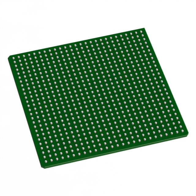
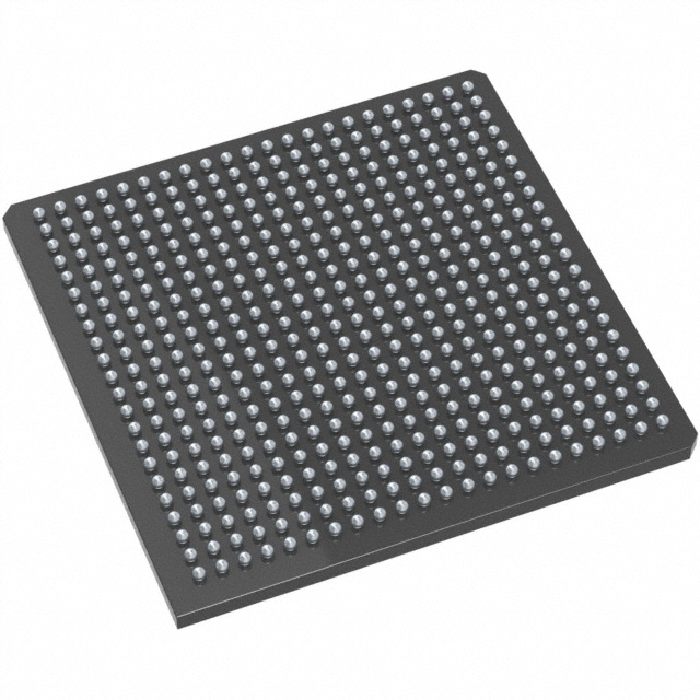
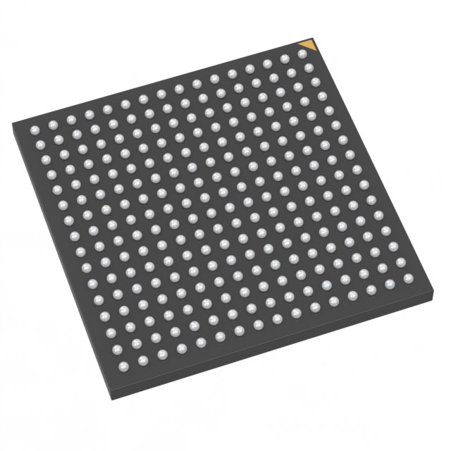
M1AFS1500-FGG484
| Part Description |
Fusion® Field Programmable Gate Array (FPGA) IC 223 276480 484-BGA |
|---|---|
| Quantity | 224 Available (as of June 15, 2026) |

| Product Category | Field Programmable Gate Array (FPGA) |
|---|---|
| Manufacturer | Microchip Technology |
| Manufacturing Status | Active |
| Manufacturer Standard Lead Time | 16 Weeks |
| Datasheet |
Specifications & Environmental
| Device Package | 484-FPBGA (23x23) | Grade | Commercial | Operating Temperature | 0°C – 85°C | ||
|---|---|---|---|---|---|---|---|
| Package / Case | 484-BGA | Number of I/O | 223 | Voltage | 1.425 V - 1.575 V | ||
| Mounting Method | Surface Mount | RoHS Compliance | ROHS3 Compliant | REACH Compliance | REACH Unaffected | ||
| Moisture Sensitivity Level | 3 (168 Hours) | Number of LABs/CLBs | 38400 | Number of Logic Elements/Cells | 38400 | ||
| Number of Gates | 1500000 | ECCN | 3A991D | HTS Code | 8542.39.0001 | ||
| Qualification | N/A | Total RAM Bits | 276480 |
Overview of M1AFS1500-FGG484 – Fusion® Field Programmable Gate Array, 223 I/O, 484-BGA
The M1AFS1500-FGG484 is a Fusion® Field Programmable Gate Array (FPGA) IC from Microchip Technology. It delivers 38,400 logic elements, approximately 0.276 Mbits of embedded memory, and 223 I/O in a compact 484-BGA package.
Designed as a commercial-grade, surface-mount FPGA, this device targets applications that require substantial on-chip logic density and a high I/O count within a constrained package and defined power and temperature envelopes.
Key Features
- Core Logic 38,400 logic elements and 1,500,000 gates provide a sizable resource pool for implementing programmable logic functions.
- Embedded Memory Approximately 0.276 Mbits of total on-chip RAM (276,480 bits) for temporary data storage and buffering.
- I/O Capacity 223 general-purpose I/O pins to support diverse peripheral and interface requirements.
- Package and Mounting 484-BGA in a 484-FPBGA (23 × 23) footprint optimized for surface-mount assembly.
- Power Supply Specified supply voltage range of 1.425 V to 1.575 V for core power planning.
- Operating Range and Grade Commercial grade with an operating temperature range of 0 °C to 85 °C.
- Environmental Compliance RoHS compliant to meet common lead-free assembly requirements.
Unique Advantages
- High logic density: 38,400 logic elements and 1.5 million gates enable substantial programmable function integration on a single device.
- Embedded on-chip RAM: Approximately 0.276 Mbits of RAM reduces reliance on external memory for intermediate data and buffering.
- Large I/O complement: 223 I/O pins support extensive peripheral interfacing without additional I/O-expanders.
- Compact BGA footprint: 484-FPBGA (23 × 23) package allows high-density board layouts while remaining surface-mount friendly.
- <strongControlled power rail: Narrow supply range (1.425–1.575 V) simplifies core power sequencing and regulation design.
- Commercial temperature suitability: Rated 0 °C to 85 °C for standard commercial deployments.
Why Choose M1AFS1500-FGG484?
The M1AFS1500-FGG484 balances substantial logic and memory resources with a high I/O count in a compact 484-BGA package, making it suitable for commercial designs that require integrated programmable logic and moderate on-chip RAM. Its defined supply voltage range and RoHS compliance aid predictable integration into production assemblies.
This Fusion® FPGA is well suited to design teams seeking a commercially rated, surface-mount programmable device that provides significant logic density and I/O capability without enlarging the PCB footprint.
Request a quote or submit an inquiry to receive pricing and availability information for the M1AFS1500-FGG484. Our team will respond with the details you need to move your design forward.


Date Founded: 1989
Headquarters: Chandler, Arizona, USA
Employees: 22,000+
Revenue: $8.349 Billion
Certifications and Memberships: ISO9001:2015, IATF16949:2016, AS 9100D


