
M1AFS1500-FGG676I
| Part Description |
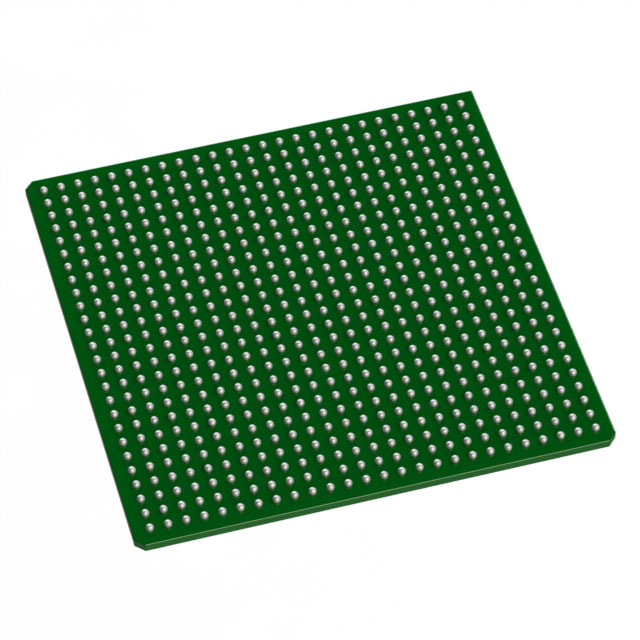
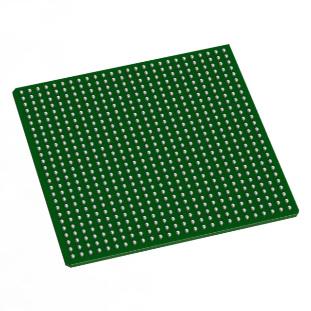
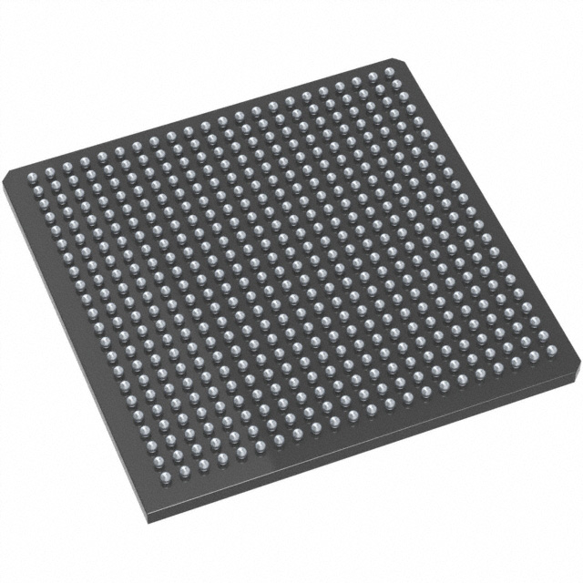
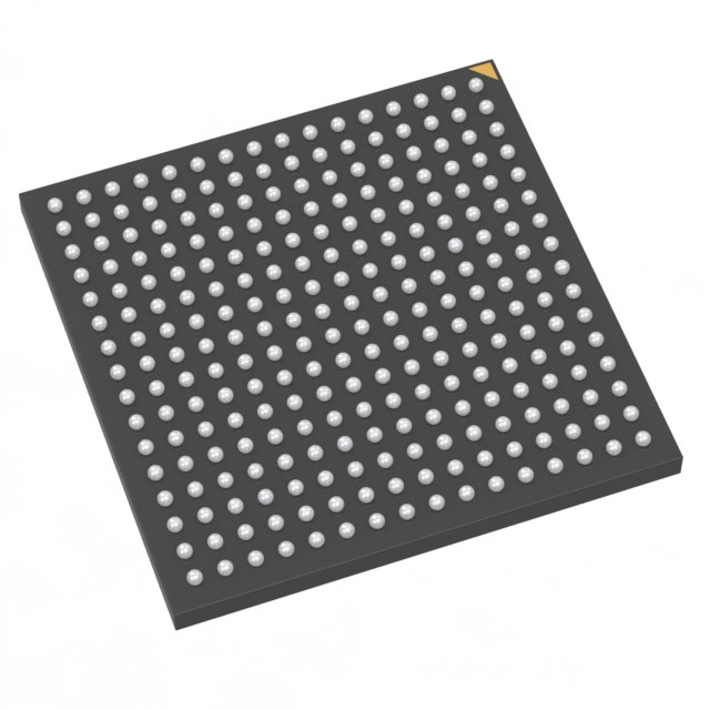
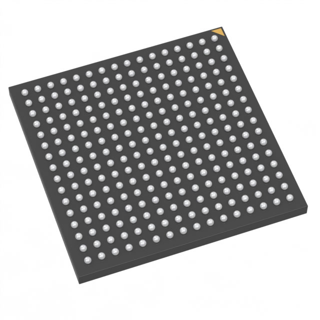
Fusion® Field Programmable Gate Array (FPGA) IC 252 276480 676-BGA |
|---|---|
| Quantity | 1,104 Available (as of October 7, 2026) |
| Product Category | Field Programmable Gate Array (FPGA) |
|---|---|
| Manufacturer | Microchip Technology |
| Manufacturing Status | Active |
| Manufacturer Standard Lead Time | 52 Weeks |
| Datasheet |
Specifications & Environmental
| Device Package | 676-FBGA (27x27) | Grade | Industrial | Operating Temperature | -40°C – 100°C | ||
|---|---|---|---|---|---|---|---|
| Package / Case | 676-BGA | Number of I/O | 252 | Voltage | 1.425 V - 1.575 V | ||
| Mounting Method | Surface Mount | RoHS Compliance | ROHS3 Compliant | REACH Compliance | REACH Unaffected | ||
| Moisture Sensitivity Level | 3 (168 Hours) | Number of LABs/CLBs | 38400 | Number of Logic Elements/Cells | 38400 | ||
| Number of Gates | 1500000 | ECCN | 3A991D | HTS Code | 8542.39.0001 | ||
| Qualification | N/A | Total RAM Bits | 276480 |
Overview of M1AFS1500-FGG676I – Fusion® FPGA, 1,500,000 gates, 38,400 logic elements, 676-BGA
The M1AFS1500-FGG676I is a Fusion® Field Programmable Gate Array (FPGA) from Microchip Technology. It provides a high-density, reprogrammable logic fabric with on-chip memory and a substantial I/O count in a compact BGA package.
Designed for industrial-grade applications, the device combines approximately 1,500,000 gates, 38,400 logic elements, and approximately 0.276 Mbits of embedded memory with a 252-pin I/O interface, a 676-FBGA (27×27) package, and an industrial operating temperature range.
Key Features
- Core Logic Provides approximately 1,500,000 gates and 38,400 logic elements for implementing complex, custom digital functions.
- Embedded Memory Approximately 276,480 bits (≈0.276 Mbits) of on-chip RAM for buffering, state storage, and small lookup tables.
- I/O Density 252 user I/O pins to support a wide range of external interfaces and signal connectivity.
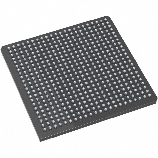
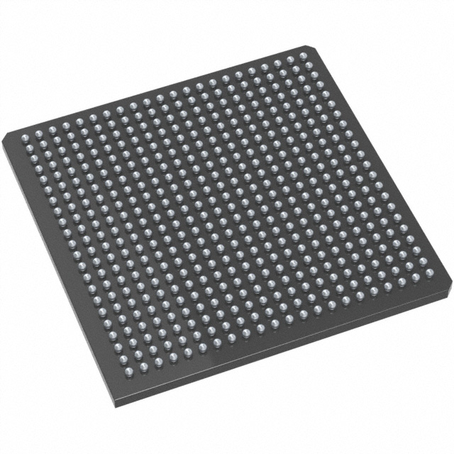
- Package & Mounting 676-FBGA (27×27) package, supplied in a 676-BGA footprint and intended for surface-mount PCB assembly.
- Power Single-core supply voltage range of 1.425 V to 1.575 V for the device core.
- Operating Range & Grade Industrial-grade device rated for operation from −40 °C to 100 °C.
- Environmental Compliance RoHS compliant.
Unique Advantages
- High logic density: The combination of ~1.5M gates and 38,400 logic elements enables substantial on-chip logic integration within a single FPGA.
- On-chip memory resource: Approximately 0.276 Mbits of embedded RAM reduces reliance on external memory for small buffers and state data.
- Generous I/O count: 252 I/O pins provide flexibility to interface with multiple peripherals, sensors, and external devices.
- Industrial temperature capability: Rated for −40 °C to 100 °C operation to meet temperature demands of industrial applications.
- Compact BGA footprint: 676-FBGA (27×27) package keeps board area low while supporting high pin count.
- Regulatory readiness: RoHS compliance supports environmental and process requirements.
Why Choose M1AFS1500-FGG676I?
The M1AFS1500-FGG676I offers a balance of high logic capacity, on-chip memory, and extensive I/O in a compact 676-BGA package, making it suitable for industrial applications that require significant programmable logic and dense signal connectivity. Its defined supply voltage range and industrial temperature rating make it straightforward to specify into designs that require predictable electrical and thermal behavior.
Backed by Microchip Technology, this Fusion® FPGA is appropriate for engineering teams and procurement groups looking for a reprogrammable, RoHS-compliant device with clear, verifiable hardware specifications for medium-to-high complexity digital designs.
Request a quote or submit an inquiry to obtain pricing and availability for the M1AFS1500-FGG676I.





















Date Founded: 1989
Headquarters: Chandler, Arizona, USA
Employees: 22,000+
Revenue: $8.349 Billion
Certifications and Memberships: ISO9001:2015, IATF16949:2016, AS 9100D




