
M1AFS600-1FGG484K
| Part Description |
Fusion® Field Programmable Gate Array (FPGA) IC 172 110592 484-BGA |
|---|---|
| Quantity | 445 Available (as of June 15, 2026) |

| Product Category | Field Programmable Gate Array (FPGA) |
|---|---|
| Manufacturer | Microchip Technology |
| Manufacturing Status | Active |
| Manufacturer Standard Lead Time | 16 Weeks |
| Datasheet |
Specifications & Environmental
| Device Package | 484-FPBGA (23x23) | Grade | Military | Operating Temperature | -55°C – 100°C | ||
|---|---|---|---|---|---|---|---|
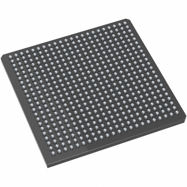
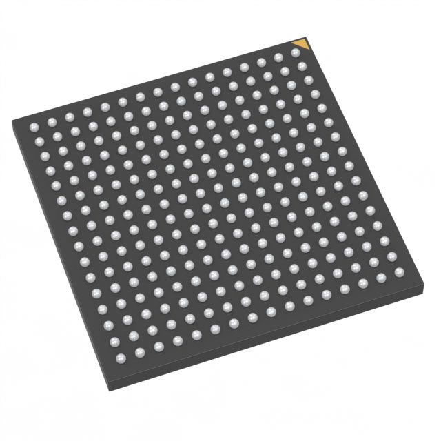
| Package / Case | 484-BGA | Number of I/O | 172 | Voltage | 1.425 V - 1.575 V | ||
| Mounting Method | Surface Mount | RoHS Compliance | ROHS3 Compliant | REACH Compliance | REACH Unaffected | ||
| Moisture Sensitivity Level | 3 (168 Hours) | Number of LABs/CLBs | 13824 | Number of Logic Elements/Cells | 13824 | ||
| Number of Gates | 600000 | ECCN | 3A991D | HTS Code | 8542.39.0001 | ||
| Qualification | N/A | Total RAM Bits | 110592 |
Overview of M1AFS600-1FGG484K – Fusion® Field Programmable Gate Array (FPGA) IC 172 110592 484-BGA
The M1AFS600-1FGG484K is a Fusion® Field Programmable Gate Array (FPGA) from Microchip Technology designed for applications that require reconfigurable digital logic in a compact ball grid array package. This device provides 13,824 logic elements, approximately 110,592 bits of on-chip RAM and 172 user I/O in a 484-ball FPBGA (23×23) surface-mount package.
With a specified supply voltage range of 1.425 V to 1.575 V and a military-grade operating temperature range of −55 °C to 100 °C, the part is suited to designs that demand robust thermal performance and long-term reliability.
Key Features
- Core Logic 13,824 logic elements (LABs/CLBs) providing programmable logic density for implementing custom digital functions and control logic.
- Gate Count Approximately 600,000 gates to support complex logic implementations and system-level integration.
- Embedded Memory 110,592 bits of on-chip RAM (approximately 0.11 Mbits) for buffering, state storage, and local data processing.
- I/O Resources 172 user I/O pins to interface with peripherals, sensors, and external logic within compact system designs.
- Package & Mounting 484-ball FPBGA (23×23) surface-mount package providing a high-density footprint for space-efficient board layouts.
- Power Nominal supply voltage specified from 1.425 V to 1.575 V to match system power-rail requirements.
- Temperature & Grade Military grade device rated for operation from −55 °C to 100 °C to meet demanding thermal environments.
- RoHS Compliance RoHS compliant to support environmental and manufacturing requirements.
Typical Applications
- Military and Defense Electronics Military-grade temperature rating and rugged specifications make this FPGA appropriate for defense systems requiring reliable reconfigurable logic.
- Rugged Embedded Systems Use the 13,824 logic elements and 172 I/O to implement custom control, signal processing, and interface logic in embedded platforms exposed to wide temperature ranges.
- Communications and Protocol Bridging Leverage the on-chip RAM and abundant I/O to implement packet buffering, protocol conversion, and custom interface logic.
- Hardware Acceleration and Custom Logic Deploy the device’s gate count and logic resources to accelerate application-specific functions and offload tasks from general-purpose processors.
Unique Advantages
- Military-Grade Reliability: Specified for −55 °C to 100 °C operation and designated as Military grade for applications with strict environmental requirements.
- Significant Logic Capacity: 13,824 logic elements and ~600,000 gates enable substantial on-chip customization without immediate need for external logic.
- On-Chip Memory for Local Data Handling: 110,592 bits of embedded RAM provide local buffering and state storage to support real-time processing tasks.
- High I/O Count in a Compact Package: 172 user I/O in a 484-FPBGA (23×23) surface-mount package simplifies routing for multi-signal systems while conserving PCB area.
- Tight Supply Voltage Specification: Defined supply range of 1.425 V to 1.575 V supports predictable power integration and system design.
- RoHS Compliant: Meets environmental compliance expectations for modern electronics manufacturing.
Why Choose M1AFS600-1FGG484K?
The M1AFS600-1FGG484K balances substantial programmable logic capacity with on-chip memory and a high I/O count in a space-efficient 484-FPBGA package. Its specified supply voltage range and military-grade temperature rating make it a practical choice for engineers designing robust, reconfigurable systems that must operate across wide thermal conditions.
This device is well suited for projects that require a combination of logic density, local memory, and numerous I/O lines, including defense, rugged embedded platforms, communications, and hardware acceleration tasks where long-term reliability and predictable electrical characteristics are important.
Request a quote or submit an inquiry to obtain pricing and availability for the M1AFS600-1FGG484K. Our team can provide the next steps for procurement and integration into your project.


Date Founded: 1989
Headquarters: Chandler, Arizona, USA
Employees: 22,000+
Revenue: $8.349 Billion
Certifications and Memberships: ISO9001:2015, IATF16949:2016, AS 9100D


