
M1AFS600-2FG256I
| Part Description |
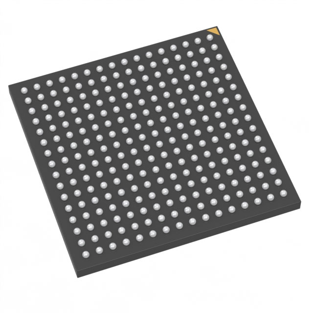
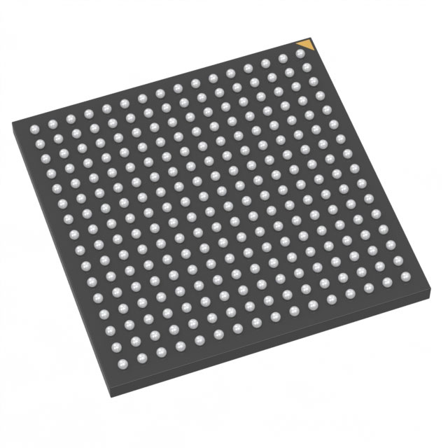
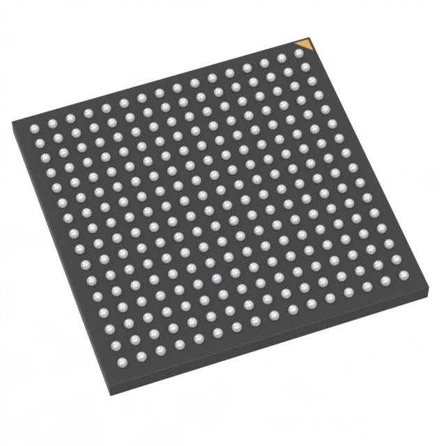
Fusion® Field Programmable Gate Array (FPGA) IC 119 110592 256-LBGA |
|---|---|
| Quantity | 540 Available (as of October 8, 2026) |
| Product Category | Field Programmable Gate Array (FPGA) |
|---|---|
| Manufacturer | Microchip Technology |
| Manufacturing Status | Active |
| Manufacturer Standard Lead Time | 16 Weeks |
| Datasheet |
Specifications & Environmental
| Device Package | 256-FPBGA (17x17) | Grade | Industrial | Operating Temperature | -40°C – 100°C | ||
|---|---|---|---|---|---|---|---|
| Package / Case | 256-LBGA | Number of I/O | 119 | Voltage | 1.425 V - 1.575 V | ||
| Mounting Method | Surface Mount | RoHS Compliance | RoHS non-compliant | REACH Compliance | REACH Unaffected | ||
| Moisture Sensitivity Level | 3 (168 Hours) | Number of LABs/CLBs | 13824 | Number of Logic Elements/Cells | 13824 | ||
| Number of Gates | 600000 | ECCN | 3A991D | HTS Code | 8542.39.0001 | ||
| Qualification | N/A | Total RAM Bits | 110592 |
Overview of M1AFS600-2FG256I – Fusion® Field Programmable Gate Array, 256-LBGA
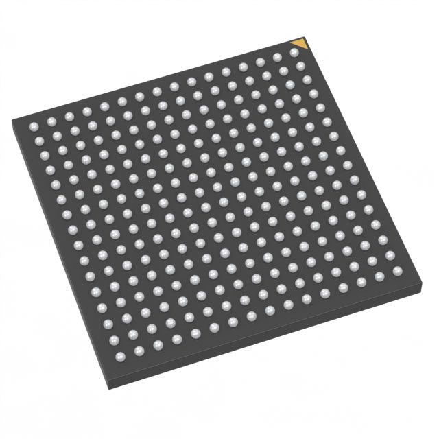
The M1AFS600-2FG256I is a Fusion® Field Programmable Gate Array (FPGA) offered in a 256-ball LFBGA package. It provides a programmable fabric with 13,824 logic elements and approximately 0.11 Mbits of embedded memory, together with 119 user I/O pins for custom digital logic and interfacing tasks.
Designed and specified for industrial use, this device supports a supply voltage range of 1.425 V to 1.575 V and an operating temperature range of −40 °C to 100 °C, making it suitable for robust embedded applications that require moderate on-chip logic, memory, and I/O integration.
Key Features
- Programmable Logic 13,824 logic elements (cells) providing flexible digital implementation capacity and support for a range of custom logic functions.
- Logic Density Approximately 600,000 gates of equivalent logic capacity to support medium-complexity designs.
- On-Chip Memory Approximately 0.11 Mbits of embedded RAM (110,592 total RAM bits) for data buffering, state storage, and small on-chip data structures.
- I/O Resources 119 user I/O pins to interface with peripherals, sensors, and external logic devices.
- Power Supply Operates from a core supply voltage between 1.425 V and 1.575 V for consistent device operation within the specified range.
- Package & Mounting Supplied in a 256-ball LBGA package (supplier package: 256-FPBGA, 17×17) and designed for surface-mount assembly.
- Industrial Temperature Range Rated for operation from −40 °C to 100 °C to meet industrial-environment thermal requirements.
- RoHS Compliant Manufactured in compliance with RoHS requirements.
Typical Applications
- Industrial control systems Use the device's 13,824 logic elements and 119 I/O pins for custom control logic, signal routing, and interfacing in industrial equipment.
- Embedded processing and glue logic Implement custom state machines, protocol bridges, and interface logic using the device’s on-chip memory and programmable fabric.
- Communications and instrumentation Leverage the device’s logic density and I/O count to implement medium-complexity protocol handling and data conditioning in instrumentation and communication modules.
Unique Advantages
- Balanced logic and memory capacity: 13,824 logic elements paired with approximately 0.11 Mbits of RAM enables compact implementations of control and data-path logic without external memory.
- Ample I/O for integration: 119 user I/Os facilitate direct connections to peripherals and sensors, reducing the need for additional interface components.
- Industrial-grade thermal range: Rated from −40 °C to 100 °C to support deployment in a wide range of industrial environments.
- Compact surface-mount package: 256-ball LBGA (256-FPBGA, 17×17) provides a high-density footprint for space-constrained boards while supporting standard surface-mount assembly.
- Narrow core-voltage window: Defined supply range (1.425 V to 1.575 V) that supports predictable power planning and design integration.
- Regulatory alignment: RoHS compliance supports use in designs that require restricted-substance conformity.
Why Choose M1AFS600-2FG256I?
The M1AFS600-2FG256I positions itself as a practical FPGA choice for engineers who need a mid-density programmable device with a balanced mix of logic, embedded memory, and I/O. Its specified industrial temperature range and RoHS compliance make it suitable for embedded and industrial projects that require reliable operation across a wide thermal envelope.
This device is well suited for designers implementing custom control logic, protocol interfaces, and moderate data-path processing where on-chip memory and a moderate number of I/Os reduce board-level complexity and component count.
Request a quote or submit an inquiry to get pricing and availability details for the M1AFS600-2FG256I. Our team can provide lead-time information and support for procurement and integration into your design.





















Date Founded: 1989
Headquarters: Chandler, Arizona, USA
Employees: 22,000+
Revenue: $8.349 Billion
Certifications and Memberships: ISO9001:2015, IATF16949:2016, AS 9100D




