
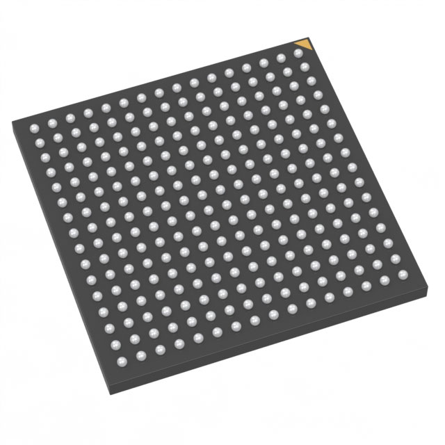
M7AFS600-2FG256I
| Part Description |
Fusion® Field Programmable Gate Array (FPGA) IC 119 110592 256-LBGA |
|---|---|
| Quantity | 1,720 Available (as of June 18, 2026) |
| Product Category | Field Programmable Gate Array (FPGA) |
|---|---|
| Manufacturer | Microchip Technology |
| Manufacturing Status | Active |
| Manufacturer Standard Lead Time | 16 Weeks |
| Datasheet |
Specifications & Environmental
| Device Package | 256-FPBGA (17x17) | Grade | Industrial | Operating Temperature | -40°C – 85°C | ||
|---|---|---|---|---|---|---|---|
| Package / Case | 256-LBGA | Number of I/O | 119 | Voltage | 1.425 V - 1.575 V | ||
| Mounting Method | Surface Mount | RoHS Compliance | RoHS non-compliant | REACH Compliance | REACH Unaffected | ||
| Moisture Sensitivity Level | 3 (168 Hours) | Number of LABs/CLBs | 13824 | Number of Logic Elements/Cells | 13824 | ||
| Number of Gates | 600000 | ECCN | 3A991D | HTS Code | 8542.39.0001 | ||
| Qualification | N/A | Total RAM Bits | 110592 |
Overview of M7AFS600-2FG256I – Fusion FPGA, 600k Gates, 119 I/Os, 256-LBGA
The M7AFS600-2FG256I is a Fusion family mixed-signal Field Programmable Gate Array (FPGA) from Microchip Technology. Built around a flash-based 130 nm process and offering 600,000 system gates with 13,824 logic elements, this device integrates digital logic, on-chip flash, embedded RAM and mixed-signal peripherals in a single surface-mount 256-LBGA package.
Designed for industrial applications that require compact, reprogrammable mixed-signal solutions, the device delivers nonvolatile instant-on operation, integrated ADCs and analog I/Os, flexible clocking and strong system security and in-system programming features to simplify board-level design and reduce BOM complexity.
Key Features
- Core Density: 600,000 system gates and 13,824 logic elements provide substantial programmable logic capacity for mid-range FPGA designs.
- Embedded Flash Memory: Approximately 4 Mbits of nonvolatile on-chip flash (two 2 Mbit blocks), plus a 1 Kbit FlashROM for configuration and code storage.
- Embedded RAM: Approximately 108 kbits of embedded SRAM organized as multiple 4,608-bit blocks with true dual-port support and programmable FIFO control logic.
- Analog Integration: Integrated multi-channel ADCs (up to 12-bit resolution, up to 600 ksps) with up to 30 scalable analog input channels, high-voltage input tolerance and dedicated gate-driver outputs for power FET control.
- On-Chip Clocking: Internal 100 MHz RC oscillator (1% accuracy), crystal oscillator support and up to six Clock Conditioning Circuits (CCCs) with one or two integrated PLLs supporting 0.75–350 MHz outputs.
- Advanced I/O: 119 I/Os with bank-selectable voltages (1.5 V, 1.8 V, 2.5 V, 3.3 V), support for single-ended and differential standards and programmable slew, drive strength and weak pull resistors.
- Security & In-System Programming: ISP capability with 128-bit AES via JTAG and FlashLock® protection to secure FPGA contents.
- Power & Low Power Modes: Single 3.3 V primary power with an on-chip 1.5 V regulator, plus sleep and standby low-power modes to support power-sensitive designs.
- Package & Environmental: Surface-mount 256-LBGA (supplier package: 256-FPBGA 17×17), industrial-grade operation from −40 °C to 85 °C, and RoHS compliant.
Typical Applications
- Industrial Control & Motor Drive: Mixed-signal integration and gate-driver outputs enable precise sensor acquisition and MOSFET control for motor control and power-conversion systems.
- Data Acquisition & Sensor Interfaces: On-chip ADC channels and analog I/Os simplify front-end designs for multi-channel sensor systems and condition monitoring.
- Embedded System Management: Nonvolatile flash, ISP with AES security and programmable clocking make the device suitable for board and module management functions in industrial platforms.
- Mezzanine & AdvancedMC Designs: Pin-compatible packages across the Fusion family and mixed-voltage I/O support mezzanine modules and AdvancedMC-style management applications.
Unique Advantages
- Highly integrated mixed-signal platform: Combines programmable logic, on-chip flash, embedded RAM and analog peripherals to reduce external components and simplify system design.
- Nonvolatile instant-on operation: Flash-based architecture retains configuration without external memory and enables immediate startup behavior after power-up.
- Flexible clocking and timing: Multiple CCCs and integrated PLLs provide versatile clock generation and conditioning for diverse system timing needs.
- Secure in-field updates: ISP with 128-bit AES and FlashLock® protection support secure firmware updates and protect intellectual property.
- Industrial temperature rating: Specified −40 °C to 85 °C operation suitable for a broad range of industrial environments.
- Scalable I/O and interfacing: Bank-selectable I/O voltages and support for differential and single-ended standards ease integration with mixed-voltage systems.
Why Choose M7AFS600-2FG256I?
The M7AFS600-2FG256I positions itself as a versatile, industrial-grade mixed-signal FPGA that consolidates logic, memory and analog peripherals into a single 256-LBGA package. With 600k gates, substantial on-chip flash and SRAM, integrated ADCs and advanced clocking, it is well suited to mid-range industrial designs that demand reprogrammability, secure in-system updates and mixed-signal integration.
Design teams building motor controls, data acquisition units, module management or mezzanine cards can leverage the Fusion architecture to reduce external BOM, simplify signal-chain design and maintain secure, field-updatable firmware over the product lifecycle.
If you would like pricing, availability or to request a quote for M7AFS600-2FG256I, please contact sales or submit a request for a quote. Our team can provide lead-time and ordering information to support your design schedule.


Date Founded: 1989
Headquarters: Chandler, Arizona, USA
Employees: 22,000+
Revenue: $8.349 Billion
Certifications and Memberships: ISO9001:2015, IATF16949:2016, AS 9100D


