
M7AFS600-2FG484I
| Part Description |
Fusion® Field Programmable Gate Array (FPGA) IC 172 110592 484-BGA |
|---|---|
| Quantity | 408 Available (as of June 14, 2026) |

| Product Category | Field Programmable Gate Array (FPGA) |
|---|---|
| Manufacturer | Microchip Technology |
| Manufacturing Status | Active |
| Manufacturer Standard Lead Time | 16 Weeks |
| Datasheet |
Specifications & Environmental
| Device Package | 484-FPBGA (23x23) | Grade | Industrial | Operating Temperature | -40°C – 85°C | ||
|---|---|---|---|---|---|---|---|
| Package / Case | 484-BGA | Number of I/O | 172 | Voltage | 1.425 V - 1.575 V | ||
| Mounting Method | Surface Mount | RoHS Compliance | RoHS non-compliant | REACH Compliance | REACH Unaffected | ||
| Moisture Sensitivity Level | 3 (168 Hours) | Number of LABs/CLBs | 13824 | Number of Logic Elements/Cells | 13824 | ||
| Number of Gates | 600000 | ECCN | 3A991D | HTS Code | 8542.39.0001 | ||
| Qualification | N/A | Total RAM Bits | 110592 |
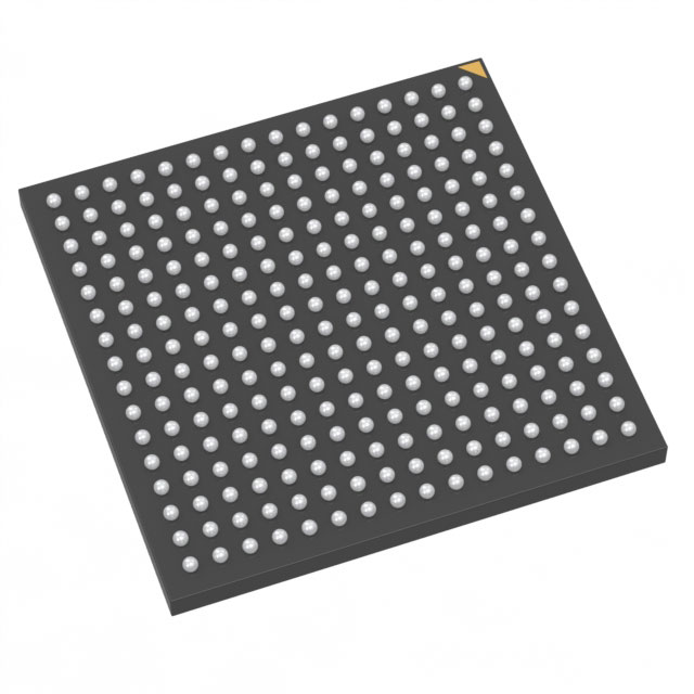
Overview of M7AFS600-2FG484I – Fusion® FPGA; 172 I/Os, 484‑BGA
The M7AFS600-2FG484I is a Fusion® family mixed-signal Field Programmable Gate Array (FPGA) in a 484‑ball BGA package. It provides 600,000 system gates and 13,824 logic elements, combined with embedded flash and analog resources to address mixed-signal and industrial control designs.
Designed for applications that require reprogrammable logic with integrated analog peripherals, this device delivers nonvolatile configuration, on-chip memory and analog I/O, and flexible bank-selectable digital I/O voltages while operating across an industrial temperature range.
Key Features
- Core Logic – 600,000 system gates and 13,824 logic elements provide a hardware fabric suitable for medium-complexity FPGA designs.
- Embedded Memory – Approximately 108 kbits (110,592 bits) of on-chip RAM and approximately 4 Mbits of embedded flash memory for code and configuration storage.
- Mixed-Signal Integration – Integrated ADC support up to 12‑bit resolution and up to 600 ksps, with up to 30 analog input channels; includes current and temperature monitor blocks and MOSFET gate driver outputs.
- High‑Performance Operation – Fusion family architecture supports up to 350 MHz system performance and includes clock conditioning circuits and integrated PLLs for flexible clock management.
- Advanced I/O – 172 user I/Os with bank-selectable voltages (1.5 V, 1.8 V, 2.5 V, 3.3 V) and support for single-ended and differential standards; built-in I/O registers and programmable drive/slew settings.
- Power and Low-Power Modes – Supports single 3.3 V power supply with an on-chip 1.5 V regulator; device core supply specified at 1.425 V to 1.575 V and includes sleep/standby low-power modes.
- In-System Programming & Security – ISP support with 128-bit AES via JTAG and FlashLock® protection for secure configuration handling.
- Package & Environmental – 484‑FPBGA (23×23) surface-mount package; industrial grade with operating temperature from −40°C to 85°C and RoHS compliance.
Typical Applications
- Power Conversion & Motor Control – On-chip MOSFET gate driver outputs, ADC channels, and current/temperature monitoring enable precise control and monitoring in power electronics and motor drives.
- Mixed-Signal Data Acquisition – Integrated ADCs and multiple analog input channels support sensor interfacing and condition monitoring where digital processing and analog measurements are required on a single device.
- Industrial Control Systems – Industrial temperature rating, flexible I/O voltages, and nonvolatile flash-based configuration make the device suitable for embedded control and automation modules.
- Embedded Logic with On-Chip Storage – Combination of logic elements, embedded RAM, and multi-megabit flash is well suited for designs that require local configuration storage and runtime data buffering.
Unique Advantages
- Highly integrated mixed-signal capability: Combines programmable logic, ADCs, gate drivers and monitoring blocks to reduce external components and simplify system design.
- Nonvolatile, instant-on operation: Flash-based configuration retains the design when powered off, enabling immediate startup without external configuration memory.
- Flexible I/O and voltage support: Bank-selectable I/O voltages and wide support for single-ended and differential standards ease interface compatibility across modules and boards.
- Security and in-system programmability: AES-protected ISP and FlashLock® provide configurable security for field updates and IP protection.
- Industrial readiness: Surface-mount 484‑FPBGA packaging, RoHS compliance and −40°C to 85°C operating range support deployment in industrial environments.
Why Choose M7AFS600-2FG484I?
The M7AFS600-2FG484I combines a medium-density programmable fabric with multi-megabit flash and extensive analog peripherals, offering a compact, mixed-signal FPGA solution for industrial control, power management, and sensor-rich applications. Its nonvolatile configuration, integrated analog resources and bank-selectable I/O voltages enable system designers to consolidate functions, reduce board-level BOM, and accelerate time to market.
This device is suited for engineers seeking a robust Fusion family FPGA with on-chip memory, ADC capability, MOSFET gate driving and secure in-system programmability, all packaged in a 484‑FPBGA for surface-mount assembly.
Request a quote or submit an inquiry to receive pricing, lead-time and availability information for the M7AFS600-2FG484I.


Date Founded: 1989
Headquarters: Chandler, Arizona, USA
Employees: 22,000+
Revenue: $8.349 Billion
Certifications and Memberships: ISO9001:2015, IATF16949:2016, AS 9100D


