
P1AFS600-2FGG256
| Part Description |
Fusion® Field Programmable Gate Array (FPGA) IC 119 110592 256-LBGA |
|---|---|
| Quantity | 185 Available (as of June 15, 2026) |
| Product Category | Field Programmable Gate Array (FPGA) |
|---|---|
| Manufacturer | Microchip Technology |
| Manufacturing Status | Active |
| Manufacturer Standard Lead Time | 16 Weeks |
| Datasheet |
Specifications & Environmental
| Device Package | 256-FPBGA (17x17) | Grade | Commercial | Operating Temperature | 0°C – 85°C | ||
|---|---|---|---|---|---|---|---|
| Package / Case | 256-LBGA | Number of I/O | 119 | Voltage | 1.425 V - 1.575 V | ||
| Mounting Method | Surface Mount | RoHS Compliance | ROHS3 Compliant | REACH Compliance | REACH Unaffected | ||
| Moisture Sensitivity Level | 3 (168 Hours) | Number of LABs/CLBs | 13824 | Number of Logic Elements/Cells | 13824 | ||
| Number of Gates | 600000 | ECCN | 3A991D | HTS Code | 8542.39.0001 | ||
| Qualification | N/A | Total RAM Bits | 110592 |
Overview of P1AFS600-2FGG256 – Fusion® Field Programmable Gate Array IC, 119 I/Os, 256-LBGA
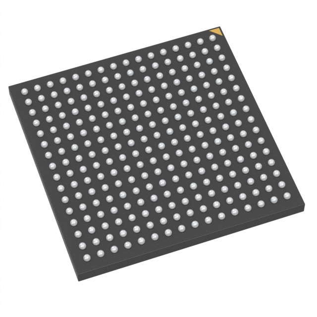
The P1AFS600-2FGG256 is a Fusion® Field Programmable Gate Array (FPGA) IC by Microchip Technology that combines mid-range logic density with on-chip memory and a broad I/O count in a compact ball-grid array package. It is specified for commercial-grade applications and is designed for surface-mount assembly in a 256-LBGA (supplier package: 256-FPBGA, 17×17) footprint.
Key on-chip resources include 13,824 logic elements, approximately 0.11 Mbits of embedded memory, and 119 general-purpose I/Os, delivering a balanced platform for configurable digital functions within a 1.425–1.575 V core supply and a 0 °C to 85 °C operating range.
Key Features
- Logic Resources Provides 13,824 logic elements (CLBs) and a gate-equivalent count of 600,000 for implementing mid-range programmable logic functions.
- Embedded Memory Approximately 0.11 Mbits of on-chip RAM (110,592 bits) for storing state, buffers, and small lookup tables directly on the FPGA fabric.
- I/O Capability 119 available I/Os to support a variety of external interfaces and peripherals in compact designs.
- Power Core voltage supply range of 1.425 V to 1.575 V to match system power design requirements.
- Package and Mounting 256-LBGA package (supplier device package: 256-FPBGA, 17×17) optimized for surface-mount PCB assembly and space-constrained boards.
- Operating Conditions Commercial-grade operation from 0 °C to 85 °C, suitable for temperature-controlled commercial products.
- Compliance RoHS-compliant design to meet modern environmental and manufacturing requirements.
Typical Applications
- Commercial Embedded Systems Use the device's 13,824 logic elements and 119 I/Os to implement custom control, glue logic, and peripheral aggregation in commercial electronics.
- Protocol Bridging and I/O Expansion Leverage the ample I/O count and on-chip memory for protocol conversion, bus interfacing, and I/O buffering tasks.
- Custom Logic Acceleration Employ the FPGA fabric to offload deterministic logic functions or small datapath acceleration within a compact 256-LBGA footprint.
Unique Advantages
- Balanced Logic and Memory: 13,824 logic elements paired with approximately 0.11 Mbits of embedded RAM provide room for both combinational and stateful designs without external memory.
- High I/O Count in a Compact Package: 119 I/Os in a 256-LBGA (17×17 FPBGA) enable dense connectivity while preserving board area.
- Commercial-Grade Reliability: Specified for 0 °C to 85 °C operation to match the requirements of mainstream commercial products.
- Controlled Core Voltage Range: A defined supply window (1.425–1.575 V) simplifies power-supply planning and system integration.
- RoHS Compliant: Supports environmental and manufacturing compliance for global commercial production.
Why Choose P1AFS600-2FGG256?
The P1AFS600-2FGG256 delivers a practical combination of logic density, embedded memory, and I/O count in a compact 256-LBGA package, tailored for commercial-grade programmable logic needs. It is well suited for designers who require mid-range FPGA resources for control, interfacing, and custom logic within a defined power and temperature envelope.
Choosing this FPGA provides a straightforward building block for commercial embedded designs that need on-chip RAM, significant I/O capability, and RoHS-compliant manufacturing, all in a surface-mount friendly form factor.
Request a quote or submit a sales inquiry to receive pricing and availability for the P1AFS600-2FGG256.


Date Founded: 1989
Headquarters: Chandler, Arizona, USA
Employees: 22,000+
Revenue: $8.349 Billion
Certifications and Memberships: ISO9001:2015, IATF16949:2016, AS 9100D


