
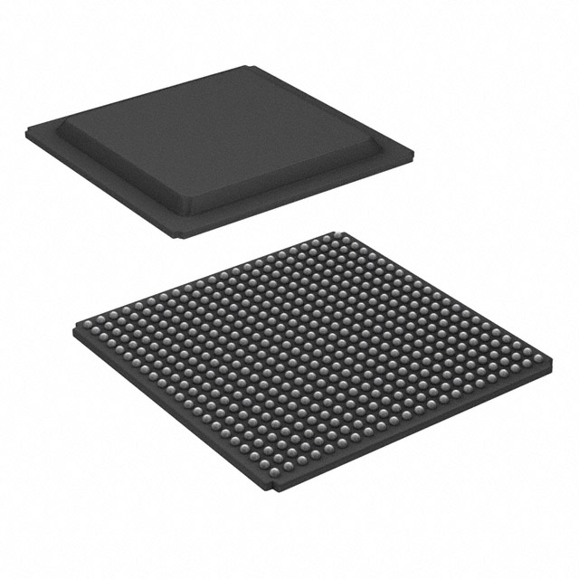
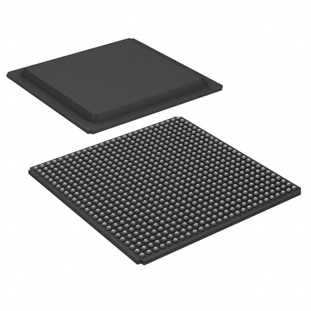
XA7K160T-1FFG676Q
| Part Description |
Kintex®-7 Field Programmable Gate Array (FPGA) IC 400 11980800 162240 676-BBGA, FCBGA |
|---|---|
| Quantity | 1,879 Available (as of June 15, 2026) |

| Product Category | Field Programmable Gate Array (FPGA) |
|---|---|
| Manufacturer | AMD |
| Manufacturing Status | Active |
| Manufacturer Standard Lead Time | 16 Weeks |
| Datasheet |
Specifications & Environmental
| Device Package | 676-FCBGA (27x27) | Grade | Automotive | Operating Temperature | -40°C – 125°C | ||
|---|---|---|---|---|---|---|---|
| Package / Case | 676-BBGA, FCBGA | Number of I/O | 400 | Voltage | 970 mV - 1.03 V | ||
| Mounting Method | Surface Mount | RoHS Compliance | ROHS3 Compliant | REACH Compliance | REACH Unaffected | ||
| Moisture Sensitivity Level | 4 (72 Hours) | Number of LABs/CLBs | 12675 | Number of Logic Elements/Cells | 162240 | ||
| Number of Gates | N/A | ECCN | 3A991D | HTS Code | 8542.39.0001 | ||
| Qualification | AEC-Q100 | Total RAM Bits | 11980800 |
Overview of XA7K160T-1FFG676Q – Kintex®-7 Automotive FPGA, 162,240 logic elements, 400 I/O, 676-FCBGA
The XA7K160T-1FFG676Q is a Kintex®-7 field programmable gate array (FPGA) optimized for high-performance, power-efficient automotive applications. Built on a 28 nm high-performance, low-power (HPL) high-k metal gate (HKMG) process, it delivers dense programmable logic alongside integrated analog and high-speed serial capabilities for system-level integration.
Designed for automotive environments, the device combines 162,240 logic elements, approximately 11.98 Mbits of embedded memory, and 400 user I/O in a 676-ball FCBGA package to support compute‑intensive and I/O‑rich designs across in‑vehicle and embedded systems.
Key Features
- Core Logic 162,240 logic elements provide a large programmable fabric for complex digital functions and custom hardware acceleration.
- On‑chip Memory Approximately 11.98 Mbits of embedded RAM and 36 Kb dual‑port block RAM primitives for on‑chip data buffering and store‑and‑forward architectures.
- DSP and Math 600 DSP48 slices support high‑throughput multiply‑accumulate operations for signal processing and accelerators.
- Analog / Mixed‑Signal (XADC) Integrated dual 12‑bit, 1 MSPS analog‑to‑digital converters with multiple channels for sensor interfacing and on‑chip monitoring.
- High‑Speed I/O and SerDes High‑performance SelectIO with DDR3 support up to 1,600 Mb/s and serial transceivers spanning 500 Mb/s to 8.0 Gb/s for high‑bandwidth links.
- Interfaces and Peripherals Integrated support for PCI Express® up to x4 Gen2 and configurable I/O standards including single‑ended and differential signaling.
- Security and Reliability On‑chip support for 256‑bit AES encryption with HMAC/SHA‑256 authentication and built‑in SEU detection and correction features.
- Power and Process 28 nm HPL HKMG process and a nominal core supply range of 0.97 V to 1.03 V for optimized performance-per-watt; datasheet notes up to 50% lower power vs. prior generation devices.
- Package and Temperature 676‑ball FCBGA (27 × 27 mm, 1.0 mm ball pitch) with automotive‑grade operating range from –40 °C to 125 °C and AEC‑Q100 qualification.
Typical Applications
- Advanced Driver Assistance Systems (ADAS) High logic density, DSP resources, and high‑speed I/O support sensor fusion, image pre‑processing, and real‑time decision logic in automotive perception stacks.
- In‑Vehicle Networking and Gateways Multi‑protocol I/O and high‑bandwidth transceivers enable aggregation, protocol bridging, and secure data transfer across vehicle domains.
- Sensor Interfacing and Data Acquisition Integrated XADC channels and flexible I/O make the device suitable for multi‑channel sensor sampling and preprocessing at the edge.
- Compute‑Intensive Embedded Systems Large logic fabric and DSP slices support custom accelerators, signal processing, and embedded compute for automotive and other ruggedized applications.
Unique Advantages
- Automotive‑Qualified Platform: AEC‑Q100 qualification and a –40 °C to 125 °C operating range make the part suitable for production automotive environments.
- High Logic Density: 162,240 logic elements allow consolidation of multiple functions into a single device, reducing system BOM and board area.
- Integrated Analog and Monitoring: Dual 12‑bit, 1 MSPS ADCs and on‑chip sensors simplify sensor interfacing and system health monitoring without external components.
- High‑Bandwidth Interfaces: SerDes up to 8.0 Gb/s and DDR3 support enable high‑throughput data paths for cameras, radar, and high‑speed peripherals.
- Security and Robustness: Built‑in AES encryption with HMAC/SHA‑256 and SEU detection/correction enhance data integrity and functional reliability.
- Power‑Efficient Process: 28 nm HPL HKMG technology and a tightly specified core voltage range deliver a balance of performance and energy efficiency.
Why Choose XA7K160T-1FFG676Q?
The XA7K160T-1FFG676Q positions itself as a high‑performance, automotive‑grade FPGA that combines substantial logic capacity, DSP horsepower, embedded analog, and high‑speed connectivity in a single package. Its process and power characteristics make it suitable for designs where compute density and thermal robustness are required.
This device is a fit for engineers building in‑vehicle compute modules, sensor processing nodes, and high‑bandwidth gateways who need a certified automotive component with a broad set of on‑chip features to reduce system complexity and accelerate time to production.
Request a quote or submit an inquiry to discuss availability and pricing for the XA7K160T-1FFG676Q and to evaluate how it fits your next design.


Date Founded: 1969
Headquarters: Santa Clara, California, USA
Employees: 25,000+
Revenue: $22.68 Billion
Certifications and Memberships: ISO9001:2015, RoHS, REACH


