
XC2V2000-6FGG676C
| Part Description |
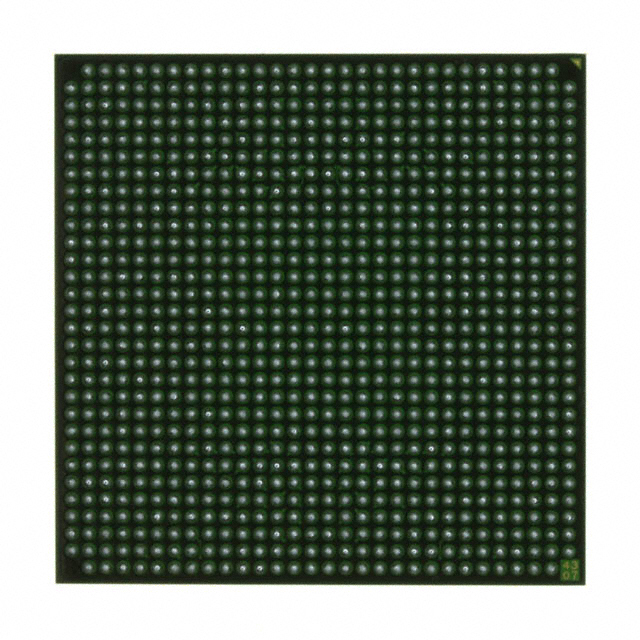
Virtex®-II Field Programmable Gate Array (FPGA) IC 456 1032192 676-BGA |
|---|---|
| Quantity | 451 Available (as of June 15, 2026) |

| Product Category | Field Programmable Gate Array (FPGA) |
|---|---|
| Manufacturer | AMD |
| Manufacturing Status | Obsolete |
| Manufacturer Standard Lead Time | Contact Us |
| Datasheet |
Specifications & Environmental
| Device Package | 676-FBGA (27x27) | Grade | Commercial | Operating Temperature | 0°C – 85°C | ||
|---|---|---|---|---|---|---|---|
| Package / Case | 676-BGA | Number of I/O | 456 | Voltage | 1.425 V - 1.575 V | ||
| Mounting Method | Surface Mount | RoHS Compliance | Unknown | REACH Compliance | REACH Unaffected | ||
| Moisture Sensitivity Level | 3 (168 Hours) | Number of LABs/CLBs | 2688 | Number of Logic Elements/Cells | 24192 | ||
| Number of Gates | 2000000 | ECCN | 3A991D | HTS Code | 8542.39.0001 | ||
| Qualification | N/A | Total RAM Bits | 1032192 |
Overview of XC2V2000-6FGG676C – Virtex®-II FPGA, 676‑BGA, 2,000,000 gates
The XC2V2000-6FGG676C is a Virtex®-II Field Programmable Gate Array (FPGA) in a 676-ball fine-pitch BGA package. This commercial-grade device delivers high-density programmable logic, abundant embedded memory and a large I/O count for I/O‑intensive and memory‑interfacing applications.
Built on the Virtex‑II platform, the device combines approximately 24,192 logic elements and roughly 1.032 Mbits of embedded memory with flexible I/O and package options to support complex digital systems and high‑bandwidth interfaces.
Key Features
- Logic Capacity Approximately 24,192 logic elements providing the programmable fabric to implement complex combinational and sequential logic.
- Embedded Memory Approximately 1.032 Mbits of on‑chip RAM (1,032,192 total RAM bits) for packet buffering, FIFO storage and local data working sets.
- Gate Count Approximately 2,000,000 system gates to quantify integration density for larger designs.
- I/O Density 456 user I/O pins to support broad external connectivity and parallel interfaces.
- Arithmetic and DSP Primitives Virtex‑II platform includes dedicated 18‑bit × 18‑bit multiplier resources and fast carry chains for arithmetic and signal‑processing tasks.
- SelectRAM™ Architecture Platform-level SelectRAM block and distributed RAM resources (series information) provide flexible on‑chip memory building blocks.
- Clock Management Platform includes Digital Clock Manager (DCM) functionality for clock de‑skew and frequency synthesis (series information).
- Package 676‑ball fine‑pitch BGA (676‑FBGA, 27 × 27 mm footprint) for surface‑mount assembly and dense board integration.
- Supply Voltage Core supply range of 1.425 V to 1.575 V to match system power rails and regulation schemes.
- Operating Range & Compliance Commercial temperature grade (0 °C to 85 °C) and RoHS compliant.
Typical Applications
- Memory Interface and Bridge Designs High I/O count and SelectRAM architecture support SDR/DDR and various SRAM/DRAM interfacing and buffering functions.
- Signal Processing and DSP Dedicated 18×18 multipliers and abundant logic resources enable fixed‑point DSP blocks, filtering and data path acceleration.
- High‑I/O Control and Glue Logic Large number of user I/Os is ideal for control plane logic, parallel buses and mixed signal interface aggregation.
Unique Advantages
- High Integration Density: Approximately 2,000,000 gates and 24,192 logic elements reduce external ASIC/FPGA counts and simplify board-level design.
- Generous Embedded Memory: About 1.032 Mbits of on‑chip RAM lowers dependence on external memory for many buffering and FIFO needs.
- Flexible I/O Count: 456 user I/Os support broad system connectivity and parallel data paths without complex external multiplexing.
- Proven Platform Features: Virtex‑II platform capabilities such as SelectRAM, DCMs and dedicated multipliers provide a familiar architecture for established tool flows (series information).
- Compact, Assembly‑Friendly Package: The 676‑FBGA (27 × 27 mm) package delivers high pin density in a compact footprint for space‑constrained PCBs.
Why Choose XC2V2000-6FGG676C?
The XC2V2000-6FGG676C positions itself as a high‑density, I/O‑rich FPGA for commercial embedded designs that require substantial logic integration, on‑chip memory and robust interfacing capability. Its combination of approximately 24,192 logic elements, roughly 1.032 Mbits of embedded RAM and 456 I/Os makes it suitable for complex control, memory interface and signal processing implementations.
Designed on the Virtex‑II platform, the device benefits from platform features such as SelectRAM block resources, dedicated multipliers and clock management primitives, offering scalability and compatibility with established FPGA development flows.
Request a quote or submit an inquiry to receive pricing and availability for the XC2V2000-6FGG676C and to discuss how it fits your next design.


Date Founded: 1969
Headquarters: Santa Clara, California, USA
Employees: 25,000+
Revenue: $22.68 Billion
Certifications and Memberships: ISO9001:2015, RoHS, REACH


