
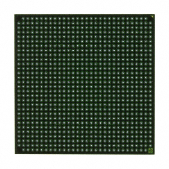
XC2V2000-6BGG575C
| Part Description |
Virtex®-II Field Programmable Gate Array (FPGA) IC 408 1032192 575-BBGA |
|---|---|
| Quantity | 389 Available (as of October 8, 2026) |

| Product Category | Field Programmable Gate Array (FPGA) |
|---|---|
| Manufacturer | AMD |
| Manufacturing Status | Obsolete |
| Manufacturer Standard Lead Time | Contact Us |
| Datasheet |
Specifications & Environmental
| Device Package | 575-BGA (31x31) | Grade | Commercial | Operating Temperature | 0°C – 85°C | ||
|---|---|---|---|---|---|---|---|
| Package / Case | 575-BBGA | Number of I/O | 408 | Voltage | 1.425 V - 1.575 V | ||
| Mounting Method | Surface Mount | RoHS Compliance | Unknown | REACH Compliance | REACH Unaffected | ||
| Moisture Sensitivity Level | 3 (168 Hours) | Number of LABs/CLBs | 2688 | Number of Logic Elements/Cells | 24192 | ||
| Number of Gates | 2000000 | ECCN | 3A991D | HTS Code | 8542.39.0001 | ||
| Qualification | N/A | Total RAM Bits | 1032192 |
Overview of XC2V2000-6BGG575C – Virtex®-II FPGA, 408 I/O, 575-BBGA
The XC2V2000-6BGG575C is a Virtex®-II Field Programmable Gate Array (FPGA) in a 575-ball BGA (31 × 31) package, designed for commercial-grade applications. Built on the Virtex-II platform architecture, it delivers a balance of logic capacity, embedded memory, and flexible I/O suitable for complex digital designs that require on-chip RAM, dedicated arithmetic blocks and a high I/O count.
This device targets designs requiring substantial programmable logic and memory integration — including memory interface controllers, DSP building blocks, and high-density I/O subsystems — while operating within a commercial temperature range.
Key Features
- Logic Capacity 2,688 CLBs providing 24,192 logic elements, enabling medium-to-high complexity logic implementation.
- Embedded Memory Approximately 1.03 Mbits of total on-chip RAM (1,032,192 bits) across block SelectRAM resources for data buffering and state storage.
- Arithmetic and DSP Resources Virtex-II platform includes dedicated 18-bit × 18-bit multipliers and fast carry logic chains for efficient arithmetic and DSP functions.
- I/O Density and Flexibility 408 user I/Os in the 575-BBGA package to support wide parallel buses, memory interfaces, and multi-channel I/O configurations.
- Clocking and Timing Virtex-II architecture provides Digital Clock Manager (DCM) and global clock resources for flexible clocking and deskewing across the design.
- Package and Mounting 575-BBGA (31 × 31) supplier device package; surface-mount mounting facilitates PCB integration in compact, high-density boards.
- Power and Supply Core voltage supply range specified at 1.425 V to 1.575 V.
- Operating Conditions Commercial grade device with an operating temperature range of 0 °C to 85 °C and RoHS compliance.
Typical Applications
- Memory Interface and Controllers Leverage the Virtex-II platform’s high-performance external memory interface support (SDR/DDR, SRAM, QDR, and CAM interfaces) for DRAM/SRAM controller implementations and memory bridge designs.
- Digital Signal Processing Use dedicated 18×18 multipliers and abundant logic elements to implement filters, transforms, and other DSP pipelines.
- High-Density I/O Systems With 408 I/Os and the 575-BBGA package, integrate wide parallel buses, multi-channel interfaces, or complex board-level I/O subsystems.
- Embedded System Glue and Bussing Combine CLBs and block SelectRAM to implement custom protocol adapters, packet buffers, and custom peripheral logic.
Unique Advantages
- Balanced Logic and Memory Integration: 2,688 CLBs paired with approximately 1.03 Mbits of embedded RAM lets you implement both control logic and substantial on-chip data storage in a single device.
- Dedicated Arithmetic Resources: On-chip 18×18 multipliers reduce external component needs for DSP workloads, simplifying BOM and improving performance density.
- High I/O Count in Compact Package: 408 user I/Os in a 575-BBGA (31 × 31) provide a dense I/O solution for complex board-level interconnect without increasing board footprint.
- Commercial Temperature and RoHS Compliance: Commercial-grade operation (0 °C to 85 °C) with RoHS-compliant materials supports standard electronics manufacturing and deployment environments.
- Virtex-II Platform Capabilities: Architectural features such as SelectRAM memory hierarchy, Digital Clock Manager, and global clock buffers provide established FPGA building blocks for reliable system design.
Why Choose XC2V2000-6BGG575C?
The XC2V2000-6BGG575C brings Virtex-II platform architecture into a mid-range FPGA offering a strong combination of logic density, embedded RAM, dedicated arithmetic resources and a high I/O count in a compact 575-BBGA package. It is well suited for commercial designs that require integrated memory, DSP capability and broad interfacing without stepping up to larger device families.
Designers and procurement teams seeking a commercially graded, RoHS-compliant FPGA with clearly defined supply and thermal ranges will find the XC2V2000-6BGG575C a practical choice for applications spanning memory interfaces, DSP functions, and board-level I/O aggregation.
Request a quote or submit your project requirements to receive pricing and availability for the XC2V2000-6BGG575C. Our team will respond with a formal quote to support your sourcing and design timelines.
























Date Founded: 1969
Headquarters: Santa Clara, California, USA
Employees: 25,000+
Revenue: $22.68 Billion
Certifications and Memberships: ISO9001:2015, RoHS, REACH











