
XC2V250-4CSG144C
| Part Description |
Virtex®-II Field Programmable Gate Array (FPGA) IC 92 442368 144-TFBGA, CSPBGA |
|---|---|
| Quantity | 1,572 Available (as of June 15, 2026) |

| Product Category | Field Programmable Gate Array (FPGA) |
|---|---|
| Manufacturer | AMD |
| Manufacturing Status | Obsolete |
| Manufacturer Standard Lead Time | Contact Us |
| Datasheet |
Specifications & Environmental
| Device Package | 144-LCSBGA (12x12) | Grade | Commercial | Operating Temperature | 0°C – 85°C | ||
|---|---|---|---|---|---|---|---|
| Package / Case | 144-TFBGA, CSPBGA | Number of I/O | 92 | Voltage | 1.425 V - 1.575 V | ||
| Mounting Method | Surface Mount | RoHS Compliance | Unknown | REACH Compliance | REACH Unaffected | ||
| Moisture Sensitivity Level | 3 (168 Hours) | Number of LABs/CLBs | 384 | Number of Logic Elements/Cells | 3456 | ||
| Number of Gates | 250000 | ECCN | 3A001A7B | HTS Code | 8542.39.0001 | ||
| Qualification | N/A | Total RAM Bits | 442368 |
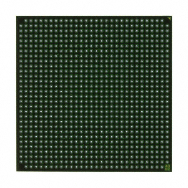
Overview of XC2V250-4CSG144C – Virtex®-II FPGA, 92 I/Os, approximately 0.42 Mbits embedded RAM, 144-TFBGA
The XC2V250-4CSG144C is a Virtex®-II field programmable gate array (FPGA) supplied in a 144-TFBGA (CSPBGA) surface-mount package. It combines a dense logic fabric with embedded memory and programmable I/O to support custom digital designs.
As part of the Virtex-II platform, the device provides on-chip block RAM, dedicated multiplier resources and clock-management features suitable for mid-range programmable logic applications in commercial-grade environments.
Key Features
- Logic Capacity — 3,456 logic elements to implement combinational and sequential logic for custom designs.
- Embedded Memory — Approximately 0.42 Mbits (442,368 bits) of on-chip RAM for data buffering, FIFOs and local storage.
- Dedicated Arithmetic — Series-level support for 18-bit × 18-bit multiplier resources for high-performance arithmetic functions.
- I/O and Package — 92 user I/Os in a 144-TFBGA (CSPBGA) package; supplied in a 144-LCSBGA (12×12) footprint for surface-mount assembly.
- Clock Management — Virtex-II platform clock-management features such as Digital Clock Manager (DCM) and global clock routing for precise clocking and phase control.
- Power and Voltage — Core supply range 1.425 V to 1.575 V to match system power rails and design constraints.
- Operating Range — Commercial-grade device rated for 0 °C to 85 °C ambient operation.
- Regulatory — RoHS compliant, supporting lead‑free assembly processes.
Typical Applications
- Memory Interface and Controller — Implement high-performance DRAM/SRAM interface logic and custom memory controllers using on-chip RAM and robust I/O resources.
- Signal Processing and DSP — Use embedded RAM and dedicated multipliers for filtering, data packing, and arithmetic acceleration in mid-range DSP tasks.
- Custom Logic and Prototyping — Rapidly prototype or deploy custom state machines, protocol bridges and glue logic leveraging the FPGA’s logic elements and programmable I/O.
- Clocked Systems — Designs that require precise clock control and phase management benefit from the Virtex-II clock management features.
Unique Advantages
- Balanced resource mix: A combination of 3,456 logic elements and approximately 0.42 Mbits of embedded RAM lets you implement control, datapath and buffering on a single device.
- Dedicated arithmetic support: On-chip 18×18 multiplier resources simplify implementation of multiply‑intensive functions without consuming general logic.
- Flexible packaging: 144-TFBGA (CSPBGA) surface-mount package with a 12×12 LCSBGA footprint enables compact board layouts while supporting 92 I/Os.
- Deterministic clocking: Platform-level clock-management features provide phase control and clock de-skew options for synchronous systems.
- Commercial-grade reliability: Specified operating range of 0 °C to 85 °C and RoHS compliance for standard commercial applications and lead‑free assembly.
- Controlled core power: Narrow core voltage range (1.425 V–1.575 V) supports stable power sequencing and predictable performance.
Why Choose XC2V250-4CSG144C?
The XC2V250-4CSG144C offers a practical balance of logic, embedded memory and arithmetic resources in a compact 144-TFBGA package. It is suited to engineers who need a commercial-grade Virtex-II FPGA with dedicated multiplier blocks, substantial on-chip RAM and flexible I/O for mid-range programmable logic tasks.
Its platform-level clock management and RoHS compliance provide design stability and manufacturing compatibility, making it a solid choice for applications that require integrated memory, arithmetic acceleration and configurable interfacing in a surface-mount FPGA solution.
Request a quote or submit an inquiry to receive pricing and availability information for the XC2V250-4CSG144C. Our team can assist with ordering and supply details tailored to your project requirements.


Date Founded: 1969
Headquarters: Santa Clara, California, USA
Employees: 25,000+
Revenue: $22.68 Billion
Certifications and Memberships: ISO9001:2015, RoHS, REACH


