
XC2V250-4CSG144I
| Part Description |
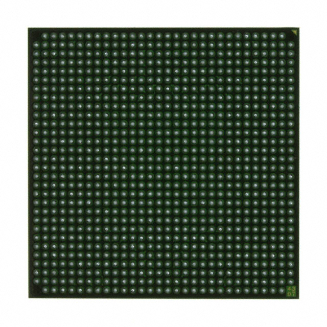
Virtex®-II Field Programmable Gate Array (FPGA) IC 92 442368 144-TFBGA, CSPBGA |
|---|---|
| Quantity | 450 Available (as of June 14, 2026) |

| Product Category | Field Programmable Gate Array (FPGA) |
|---|---|
| Manufacturer | AMD |
| Manufacturing Status | Obsolete |
| Manufacturer Standard Lead Time | Contact Us |
| Datasheet |
Specifications & Environmental
| Device Package | 144-LCSBGA (12x12) | Grade | Industrial | Operating Temperature | -40°C – 100°C | ||
|---|---|---|---|---|---|---|---|
| Package / Case | 144-TFBGA, CSPBGA | Number of I/O | 92 | Voltage | 1.425 V - 1.575 V | ||
| Mounting Method | Surface Mount | RoHS Compliance | Unknown | REACH Compliance | REACH Unaffected | ||
| Moisture Sensitivity Level | 3 (168 Hours) | Number of LABs/CLBs | 384 | Number of Logic Elements/Cells | 3456 | ||
| Number of Gates | 250000 | ECCN | 3A001A7B | HTS Code | 8542.39.0001 | ||
| Qualification | N/A | Total RAM Bits | 442368 |
Overview of XC2V250-4CSG144I – Virtex®-II FPGA, 3,456 logic elements, 144-TFBGA
The XC2V250-4CSG144I is a Virtex®-II field programmable gate array (FPGA) manufactured by AMD, supplied in a 144-TFBGA/CSPBGA package. It delivers a balance of programmable logic, on-chip memory and I/O capability suited to industrial applications that require reconfigurable logic and robust operating conditions.
Built on the Virtex-II platform, the device targets designs needing moderate logic density, embedded memory and flexible interfacing while supporting industrial temperature ranges and controlled supply voltage for reliable operation.
Key Features
- Logic Capacity — 3,456 logic elements (reported as 3,456 logic cells) and approximately 250,000 gates provide the programmable fabric for combinational and sequential logic.
- Embedded Memory — Approximately 0.44 Mbits (442,368 bits) of on-chip RAM to support buffers, FIFOs and small embedded storage needs.
- I/O Count and Flexibility — 92 user I/O pins available for interface to peripherals, memory and custom I/O networks.
- Arithmetic Resources — Series-level Virtex-II features include dedicated 18-bit × 18-bit multiplier blocks for hardware acceleration of DSP and arithmetic functions.
- Clock Management — Virtex-II platform supports Digital Clock Manager (DCM) modules for clock de-skew and frequency synthesis (series-level capability).
- Package and Mounting — Surface-mount 144-TFBGA (supplier package: 144-LCSBGA, 12×12) for high-density board integration.
- Power Supply — Specified core voltage range of 1.425 V to 1.575 V for regulated, predictable power design.
- Industrial Temperature Grade — Qualified for operation from −40 °C to 100 °C to meet demanding environmental conditions.
- Compliance — RoHS compliant, supporting regulatory and manufacturing requirements.
Typical Applications
- Industrial Automation — Implement motor control, logic sequencing and custom protocol handling using the device’s logic and I/O resources within industrial temperature limits.
- Memory Interface and Buffering — Use embedded RAM and series-level high-performance memory interfaces to implement DRAM/SDRAM buffering, caching or interface glue logic.
- Signal Processing Acceleration — Leverage on-chip multipliers and logic fabric for finite impulse response (FIR) filters, fixed-point arithmetic and other DSP blocks.
- Custom I/O and Protocol Bridging — 92 I/Os enable implementation of custom peripheral interfaces, bus bridging and board-level glue logic.
Unique Advantages
- Balanced Logic and Memory: Combines ~3,456 logic elements with approximately 0.44 Mbits of embedded RAM to support control, buffering and moderate DSP tasks without external devices.
- Industrial Temperature Range: Rated from −40 °C to 100 °C for reliable deployment in harsh operating environments.
- Compact, High-Density Package: 144-TFBGA (12×12) BGA footprint minimizes board area while offering robust soldered connections for production assemblies.
- Deterministic Power Envelope: Defined core supply range (1.425 V–1.575 V) simplifies power rail design and margining for stable operation.
- Series-Proven Platform Features: Access to Virtex-II platform capabilities such as 18×18 multipliers and Digital Clock Manager modules for clocking and arithmetic acceleration.
Why Choose XC2V250-4CSG144I?
The XC2V250-4CSG144I brings Virtex®-II platform capabilities into a compact, industrial-grade package, delivering a useful combination of logic density, embedded memory and configurable I/O for mid-range FPGA applications. Its defined electrical and thermal specifications support predictable integration into industrial and embedded systems.
This part is appropriate for designers who need moderate gate count and on-chip RAM with the flexibility of reprogrammable logic, placed within a robust package and temperature envelope that aligns with industrial system requirements.
Request a quote or submit an inquiry to receive pricing, availability and technical support information for the XC2V250-4CSG144I.


Date Founded: 1969
Headquarters: Santa Clara, California, USA
Employees: 25,000+
Revenue: $22.68 Billion
Certifications and Memberships: ISO9001:2015, RoHS, REACH


