
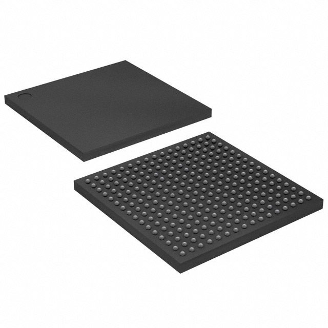
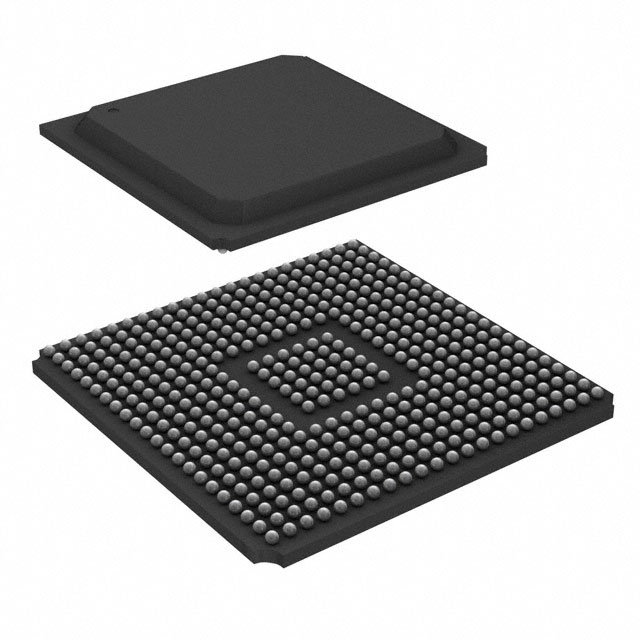
XC2V500-5FGG256I
| Part Description |
Virtex®-II Field Programmable Gate Array (FPGA) IC 172 589824 256-BGA |
|---|---|
| Quantity | 584 Available (as of June 14, 2026) |

| Product Category | Field Programmable Gate Array (FPGA) |
|---|---|
| Manufacturer | AMD |
| Manufacturing Status | Obsolete |
| Manufacturer Standard Lead Time | Contact Us |
| Datasheet |
Specifications & Environmental
| Device Package | 256-FBGA (17x17) | Grade | Industrial | Operating Temperature | -40°C – 100°C | ||
|---|---|---|---|---|---|---|---|
| Package / Case | 256-BGA | Number of I/O | 172 | Voltage | 1.425 V - 1.575 V | ||
| Mounting Method | Surface Mount | RoHS Compliance | Unknown | REACH Compliance | REACH Unaffected | ||
| Moisture Sensitivity Level | 3 (168 Hours) | Number of LABs/CLBs | 768 | Number of Logic Elements/Cells | 6912 | ||
| Number of Gates | 500000 | ECCN | 3A001A7B | HTS Code | 8542.39.0001 | ||
| Qualification | N/A | Total RAM Bits | 589824 |
Overview of XC2V500-5FGG256I – Virtex®-II Field Programmable Gate Array, 172 I/O, ~0.59 Mbits RAM, 256-BGA
The XC2V500-5FGG256I is a Virtex®-II Field Programmable Gate Array (FPGA) offered in a 256-ball fine-pitch BGA package. It delivers a mid-range FPGA fabric with 6,912 logic elements (768 CLBs), approximately 0.59 Mbits of embedded memory and roughly 500,000 system gates, targeted at applications requiring configurable logic, on-chip RAM and substantial I/O.
Built on the Virtex-II platform architecture, this device is suitable for designs needing high I/O density, dedicated arithmetic resources and flexible clock management while operating across an industrial temperature range.
Key Features
- Logic Capacity — 6,912 logic elements (768 CLBs) providing programmable fabric for combinational and sequential logic implementations.
- Embedded Memory — Total on-chip RAM of 589,824 bits (approximately 0.59 Mbits) for data buffering, FIFOs and distributed memory functions.
- Arithmetic Resources — Series-level support for 18-bit × 18-bit multiplier blocks to accelerate fixed-point and DSP arithmetic (feature included in the Virtex-II platform).
- I/O — 172 user I/O pins to interface with external peripherals and memory devices.
- Clock Management — Digital Clock Manager (DCM) functionality available on the Virtex-II platform for precise deskew, frequency synthesis and phase control.
- Package & Mounting — 256-ball fine-pitch BGA (256-FBGA, 17 × 17) package; surface-mount mounting type for board-level integration.
- Power — Core voltage supply range of 1.425 V to 1.575 V to match system power domains.
- Industrial Temperature Grade — Rated for operation from −40 °C to 100 °C to support industrial environments.
- Regulatory — RoHS-compliant manufacturing.
- Platform Support — Supported by the Virtex-II platform development ecosystem and documentation for design and configuration workflows.
Typical Applications
- High-performance memory interfaces — Use the device’s I/O density and on-chip RAM to implement SDR/DDR or SRAM interface logic and buffering in memory controller designs.
- Digital signal processing — Leverage the embedded RAM and series-level 18×18 multiplier resources for fixed-point DSP kernels, filtering and data transformation tasks.
- Communication and networking — Deploy the configurable logic and abundant I/O for protocol handling, packet buffering and interface bridging in networking equipment.
- System prototyping and integration — Provide a programmable integration point for custom logic, glue functions and system-level validation using the Virtex-II toolchain support.
Unique Advantages
- Balanced logic and memory — Combines 6,912 logic elements with approximately 0.59 Mbits of embedded RAM to support control logic alongside substantial data storage on-chip.
- Significant I/O count — 172 user I/Os enable direct interfacing to a wide range of peripherals and external memories, reducing external glue logic.
- Industrial temperature range — Rated from −40 °C to 100 °C for reliable operation across demanding environmental conditions.
- Compact BGA package — 256-FBGA (17 × 17) delivers a small board footprint for space-constrained applications while maintaining routing density.
- Low-voltage core — Operates with a core voltage window of 1.425 V to 1.575 V to align with modern power domains and reduce power delivery overhead.
- Standards-driven platform support — Backed by the Virtex-II platform documentation and development tools to accelerate implementation and debugging.
Why Choose XC2V500-5FGG256I?
The XC2V500-5FGG256I positions itself as a practical mid-range Virtex®-II FPGA that balances logic capacity, embedded memory and I/O for systems requiring configurable hardware acceleration, memory interfacing and protocol handling. Its industrial temperature rating and RoHS compliance make it suitable for long-term deployment in industrial and embedded applications.
Designers benefit from the Virtex-II platform features—such as dedicated arithmetic blocks, SelectRAM memory hierarchy and clock management—combined with the device’s package and electrical specifications to build robust, scalable solutions with established toolchain support.
Request a quote or submit an inquiry to receive pricing, availability and technical support for the XC2V500-5FGG256I. Our team can assist with lead times and volume options to help move your design forward.


Date Founded: 1969
Headquarters: Santa Clara, California, USA
Employees: 25,000+
Revenue: $22.68 Billion
Certifications and Memberships: ISO9001:2015, RoHS, REACH


