
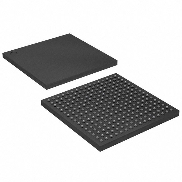
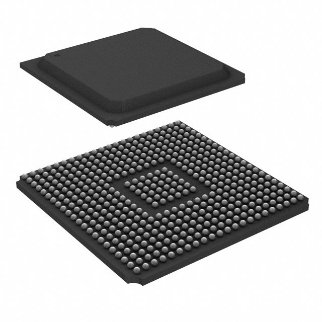
XC2V500-5FG256I
| Part Description |
Virtex®-II Field Programmable Gate Array (FPGA) IC 172 589824 256-BGA |
|---|---|
| Quantity | 798 Available (as of June 9, 2026) |
| Product Category | Field Programmable Gate Array (FPGA) |
|---|---|
| Manufacturer | AMD |
| Manufacturing Status | Obsolete |
| Manufacturer Standard Lead Time | Contact Us |
| Datasheet |
Specifications & Environmental
| Device Package | 256-FBGA (17x17) | Grade | Industrial | Operating Temperature | -40°C – 100°C | ||
|---|---|---|---|---|---|---|---|
| Package / Case | 256-BGA | Number of I/O | 172 | Voltage | 1.425 V - 1.575 V | ||
| Mounting Method | Surface Mount | RoHS Compliance | RoHS non-compliant | REACH Compliance | REACH Unaffected | ||
| Moisture Sensitivity Level | 3 (168 Hours) | Number of LABs/CLBs | 768 | Number of Logic Elements/Cells | 6912 | ||
| Number of Gates | 500000 | ECCN | EAR99 | HTS Code | 8542.39.0001 | ||
| Qualification | N/A | Total RAM Bits | 589824 |
Overview of XC2V500-5FG256I – Virtex®-II Field Programmable Gate Array, 172 I/O, 256-BGA
The XC2V500-5FG256I is a Virtex®-II platform FPGA supplied in a 256-ball fine-pitch BGA (17 × 17 mm FBGA) package. Designed for industrial-temperature deployments, this device integrates configurable logic, embedded memory, and high-performance I/O in a surface-mount form factor.
Targeted at designs that require flexible logic resources, on-chip RAM, and robust clocking and arithmetic support, the device is suitable for applications demanding reconfigurable hardware with precision timing and multiple I/O interfaces. It ships RoHS compliant and operates across an extended voltage and temperature range to support industrial systems.
Key Features
- Logic Resources — 768 CLBs (configurable logic blocks) providing 6,912 logic elements/cells and approximately 500,000 gates for implementing custom digital logic.
- Embedded Memory — Approximately 0.59 Mbits (589,824 bits) of on-chip RAM to support buffering, lookup tables, and state storage within logic designs.
- Dedicated Arithmetic Blocks — Series-level Virtex®-II architecture includes dedicated multiplier resources for high-throughput arithmetic (as described in the Virtex-II product specification).
- High-Performance I/O — 172 user I/O pins (package-limited) supporting high-speed interfaces and diverse signaling standards described in the Virtex®-II platform documentation.
- Clock Management — Device family features Digital Clock Manager (DCM) and global clock routing options for precise clock de-skew and flexible frequency management (per Virtex®-II platform specification).
- Package and Mounting — 256-BGA (256-FBGA, 17×17 mm) package optimized for surface-mount assembly and compact system integration.
- Electrical and Environmental — Supply voltage 1.425 V to 1.575 V, industrial operating temperature range −40 °C to 100 °C, and RoHS compliant.
Typical Applications
- Memory Interface and Bridging — Implement SDR/DDR memory controllers and interface logic using the device’s on-chip RAM and high-performance I/O.
- Signal Processing and DSP — Use dedicated multiplier blocks and the available logic fabric for filtering, transform engines, and real-time arithmetic workloads.
- Prototyping and Custom Logic — Rapidly implement and iterate custom digital functions, state machines, and control logic with abundant logic elements and embedded memory.
- High-Speed I/O Integration — Aggregate and route multiple high-bandwidth serial or parallel interfaces using the device’s extensive I/O resources and platform clocking features.
Unique Advantages
- Configurable, Deterministic Logic: 768 CLBs and 6,912 logic elements/cells provide a predictable resource set for complex finite-state machines and data-path implementations.
- On-Chip Memory for Low-Latency Tasks: Approximately 0.59 Mbits of embedded RAM reduces external memory dependence for buffering and tight-loop processing.
- Industrial Temperature Range: −40 °C to 100 °C operation supports deployment in industrial environments without derating logic or I/O capability.
- Compact Surface-Mount Package: 256-FBGA (17×17 mm) enables high-density board layouts while maintaining 172 user I/Os for system connectivity.
- Controlled Supply Range: Narrow supply window (1.425 V–1.575 V) helps designers manage power rails and ensure stable core operation in system designs.
- Regulatory and Supply Confidence: RoHS compliance supports environmentally conscious manufacturing and downstream regulatory requirements.
Why Choose XC2V500-5FG256I?
The XC2V500-5FG256I brings together a Virtex®-II FPGA architecture with a balanced set of logic, embedded memory, and I/O resources in a compact 256-FBGA package. Its industrial-grade temperature range and controlled core voltage make it a practical choice for embedded system designers who need reprogrammable hardware with reliable environmental performance.
This device suits teams building memory interfaces, DSP blocks, custom control logic, or multi-interface bridging where predictable logic resources and on-chip RAM simplify board-level design and reduce external component count. Backed by the Virtex®-II family documentation and platform features, it offers a stable foundation for mid-density FPGA applications.
Request a quote or submit an inquiry to receive pricing, availability, and technical support for the XC2V500-5FG256I. Our team can provide lead-time details and assistance with part selection for your design requirements.


Date Founded: 1969
Headquarters: Santa Clara, California, USA
Employees: 25,000+
Revenue: $22.68 Billion
Certifications and Memberships: ISO9001:2015, RoHS, REACH


