
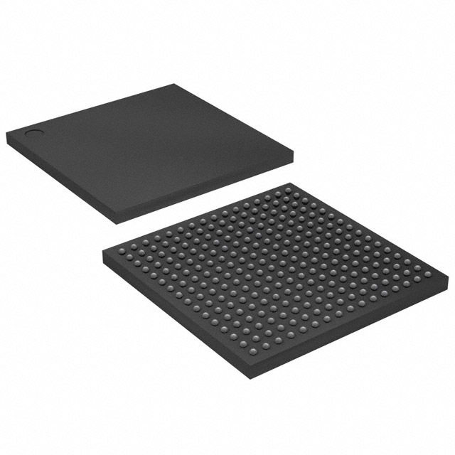
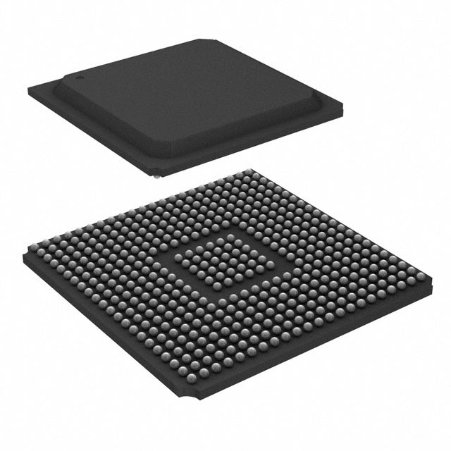
XC2V500-4FGG256C
| Part Description |
Virtex®-II Field Programmable Gate Array (FPGA) IC 172 589824 256-BGA |
|---|---|
| Quantity | 42 Available (as of June 15, 2026) |

| Product Category | Field Programmable Gate Array (FPGA) |
|---|---|
| Manufacturer | AMD |
| Manufacturing Status | Obsolete |
| Manufacturer Standard Lead Time | Contact Us |
| Datasheet |
Specifications & Environmental
| Device Package | 256-FBGA (17x17) | Grade | Commercial | Operating Temperature | 0°C – 85°C | ||
|---|---|---|---|---|---|---|---|
| Package / Case | 256-BGA | Number of I/O | 172 | Voltage | 1.425 V - 1.575 V | ||
| Mounting Method | Surface Mount | RoHS Compliance | Unknown | REACH Compliance | REACH Unaffected | ||
| Moisture Sensitivity Level | 3 (168 Hours) | Number of LABs/CLBs | 768 | Number of Logic Elements/Cells | 6912 | ||
| Number of Gates | 500000 | ECCN | 3A001A7B | HTS Code | 8542.39.0001 | ||
| Qualification | N/A | Total RAM Bits | 589824 |
Overview of XC2V500-4FGG256C – Virtex®-II Field Programmable Gate Array (FPGA) IC 172 589824 256-BGA
The XC2V500-4FGG256C is a Virtex®-II platform FPGA from AMD in a 256-ball fine-pitch BGA (256-FBGA, 17×17) surface-mount package. It delivers reconfigurable logic resources, embedded memory, and programmable I/O in a commercial-grade device designed for designs requiring on-chip RAM, DSP primitives, and flexible interfacing.
Key device-level specifications include 6,912 logic elements, approximately 0.59 Mbits of embedded memory, 172 user I/Os, and an operating voltage range of 1.425 V to 1.575 V with an operating temperature of 0 °C to 85 °C. The device is RoHS compliant and packaged for compact surface-mount integration.
Key Features
- Logic Capacity 6,912 logic elements and approximately 500,000 system gates provide a solid foundation for mid-range reconfigurable logic and control functions.
- Embedded Memory Approximately 0.59 Mbits (589,824 bits) of on-chip RAM for buffering, packet storage, and state machines.
- I/O and Interface Flexibility 172 user I/Os in the 256-BGA package support a wide range of external interfaces; the Virtex-II platform includes SelectIO™-Ultra and Digitally Controlled Impedance (DCI) I/O features at the family level.
- Arithmetic/DSP Resources Family-level dedicated 18-bit × 18-bit multiplier blocks provide hardware-accelerated arithmetic for signal processing and DSP algorithms.
- Clock Management Virtex-II platform clock-management features (including Digital Clock Manager modules and global clock multiplexer buffers at the family level) enable flexible clocking and precise de-skew within designs.
- Package and Power 256-FBGA (17×17) surface-mount package; nominal supply range 1.425 V to 1.575 V for core operation.
- Operating Range and Compliance Commercial grade device with an operating temperature range of 0 °C to 85 °C and RoHS compliance.
Typical Applications
- Memory interface controllers — Implement SDR/DDR and other external memory interfaces using on-chip logic and the Virtex-II family’s high-performance memory interfacing features.
- DSP and signal processing — Use embedded RAM and 18×18 multiplier blocks for FIR filters, transforms, and real-time processing tasks.
- Custom logic and protocol bridging — Create application-specific accelerators, protocol translators, and glue logic with mid-range gate count and plentiful I/O.
- Embedded control and state machines — Ideal for managing peripheral control, data aggregation, and deterministic logic functions within a compact BGA package.
Unique Advantages
- Highly integrated solution: Combines 6,912 logic elements with on-chip RAM and DSP resources to reduce external components and simplify board-level design.
- Flexible I/O capability: 172 user I/Os in a 256-FBGA package, with family-level SelectIO and DCI features to support varied interface standards and impedance requirements.
- Embedded memory for buffering: Approximately 0.59 Mbits of on-chip RAM enables efficient data storage and rapid local access for timing-critical operations.
- Dedicated arithmetic blocks: 18-bit × 18-bit multipliers at the family level accelerate multiply-intensive workloads and DSP algorithms.
- Compact, surface-mount package: 256-FBGA (17×17) provides a space-efficient footprint for mid-density FPGA implementations.
- Commercial-grade and RoHS compliant: Designed for commercial applications with environmental compliance documented.
Why Choose XC2V500-4FGG256C?
The XC2V500-4FGG256C delivers a balanced combination of reconfigurable logic, embedded memory, DSP primitives, and flexible I/O in a compact 256-BGA surface-mount package. It is well suited to mid-range FPGA designs that require on-chip RAM, dedicated multipliers, and a sizeable number of user I/Os while operating within commercial temperature ranges.
This device is appropriate for design teams and OEMs targeting compact, reconfigurable hardware for interfacing, acceleration, and control tasks. Its family-level Virtex-II features—such as SelectRAM, dedicated multipliers, and clock management capabilities—provide a scalable platform backed by established design flows and documentation.
Request a personalized quote or submit an inquiry to our team to discuss availability, lead times, and volume pricing for the XC2V500-4FGG256C.


Date Founded: 1969
Headquarters: Santa Clara, California, USA
Employees: 25,000+
Revenue: $22.68 Billion
Certifications and Memberships: ISO9001:2015, RoHS, REACH


