
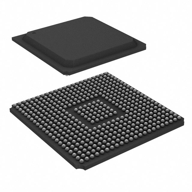
XC2V500-6FGG256C
| Part Description |
Virtex®-II Field Programmable Gate Array (FPGA) IC 172 589824 256-BGA |
|---|---|
| Quantity | 182 Available (as of October 7, 2026) |

| Product Category | Field Programmable Gate Array (FPGA) |
|---|---|
| Manufacturer | AMD |
| Manufacturing Status | Obsolete |
| Manufacturer Standard Lead Time | Contact Us |
| Datasheet |
Specifications & Environmental
| Device Package | 256-FBGA (17x17) | Grade | Commercial | Operating Temperature | 0°C – 85°C | ||
|---|---|---|---|---|---|---|---|
| Package / Case | 256-BGA | Number of I/O | 172 | Voltage | 1.425 V - 1.575 V | ||
| Mounting Method | Surface Mount | RoHS Compliance | Unknown | REACH Compliance | REACH Unaffected | ||
| Moisture Sensitivity Level | 3 (168 Hours) | Number of LABs/CLBs | 768 | Number of Logic Elements/Cells | 6912 | ||
| Number of Gates | 500000 | ECCN | 3A001A7B | HTS Code | 8542.39.0001 | ||
| Qualification | N/A | Total RAM Bits | 589824 |
Overview of XC2V500-6FGG256C – Virtex®-II FPGA, 256-BGA, 172 I/O
The XC2V500-6FGG256C is a Virtex®-II field programmable gate array supplied by AMD. It provides a balanced combination of on-chip logic, embedded memory, dedicated arithmetic resources and high-density I/O in a compact 256-ball BGA package for commercial-grade designs.
Ideal for designs that require flexible, reprogrammable logic—such as interface bridging, memory controllers and arithmetic-heavy datapaths—this device offers verified Virtex‑II platform capabilities including embedded RAM, hardware multipliers and advanced clock management.
Key Features
- Logic Capacity — 6,912 logic elements (logic cells) enabling mid-range custom logic implementations and glue-logic consolidation.
- Embedded Memory — Approximately 0.59 Mbits of on-chip RAM (589,824 total RAM bits) for buffering, FIFOs and small shared memories.
- Dedicated Arithmetic Blocks — Includes dedicated 18-bit × 18-bit multiplier resources for hardware-accelerated DSP and signal processing functions.
- I/O Resources — 172 user I/O pins supporting high-density external interfacing and protocol bridging needs.
- Clock and Timing — Digital Clock Manager (DCM) functionality from the Virtex‑II family for precise clock de-skew, frequency synthesis and phase control.
- Routing and Architecture — Virtex‑II platform routing and architecture features for predictable routing delay and scalable design implementation.
- Package and Mounting — 256-ball fine-pitch BGA (256-FBGA, 17×17) in a surface-mount package for compact board integration.
- Electrical — Core supply range specified at 1.425 V to 1.575 V for device power planning.
- Operating Range — Commercial temperature grade with an operating range of 0 °C to 85 °C.
- Compliance — RoHS compliant.
- Gate Count — 500,000 system gates to size overall design scale and resource planning.
Typical Applications
- Memory Interface & Controller Design — High-performance interfaces to external memory (SDR/DDR, SRAM families) using on-chip logic and dedicated timing resources for data path control and buffering.
- Signal Processing & DSP Blocks — Use of 18×18 multipliers and embedded RAM to implement arithmetic-heavy datapaths, filters and acceleration blocks.
- Protocol Bridging & High‑Speed I/O — 172 I/Os and Virtex‑II SelectIO capabilities enable implementation of bus bridges, protocol adapters and I/O aggregation functions.
- Custom Control & Glue Logic — Consolidate discrete ASIC/PLD functions into a reprogrammable fabric to reduce BOM and simplify board design.
Unique Advantages
- Balanced integration: Logic, embedded RAM and multipliers in a single device reduce external component count and simplify board-level design.
- Deterministic timing support: Virtex‑II clock management (DCM) features help implement reliable, phase‑controlled clocking for synchronous systems.
- Compact footprint: 256-FBGA (17×17) package offers high I/O density in a small, surface-mount package for space-constrained applications.
- Commercial-ready: Specified for 0 °C to 85 °C operation and RoHS compliant for mainstream electronics products.
- Clear power envelope: Defined core supply range (1.425 V–1.575 V) simplifies power-supply selection and design validation.
- Proven platform features: Series-level Virtex‑II capabilities—such as block SelectRAM hierarchy and dedicated multipliers—support a wide range of embedded functions without speculative claims.
Why Choose XC2V500-6FGG256C?
The XC2V500-6FGG256C is positioned for designers who need a mid-density Virtex‑II FPGA with substantial on‑chip memory, dedicated multiplier resources and a high count of user I/Os in a compact BGA footprint. Its commercial temperature rating and RoHS compliance make it suitable for a broad set of mainstream electronic products where reprogrammability, integration and predictable timing are priorities.
With 6,912 logic elements, approximately 0.59 Mbits of embedded RAM and the Virtex‑II family feature set, this device supports scalable designs that require both logic and arithmetic capabilities while keeping board area and external component count under control.
Request a quote or submit a product inquiry to receive pricing, availability and technical assistance for the XC2V500-6FGG256C.

























Date Founded: 1969
Headquarters: Santa Clara, California, USA
Employees: 25,000+
Revenue: $22.68 Billion
Certifications and Memberships: ISO9001:2015, RoHS, REACH











