
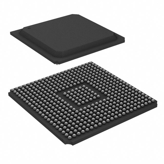
XC2V6000-4BF957C
| Part Description |
Virtex®-II Field Programmable Gate Array (FPGA) IC 684 2654208 957-BBGA, FCBGA |
|---|---|
| Quantity | 1,483 Available (as of June 16, 2026) |

| Product Category | Field Programmable Gate Array (FPGA) |
|---|---|
| Manufacturer | AMD |
| Manufacturing Status | Obsolete |
| Manufacturer Standard Lead Time | Contact Us |
| Datasheet |
Specifications & Environmental
| Device Package | 957-FCBGA (40x40) | Grade | Commercial | Operating Temperature | 0°C – 85°C | ||
|---|---|---|---|---|---|---|---|
| Package / Case | 957-BBGA, FCBGA | Number of I/O | 684 | Voltage | 1.425 V - 1.575 V | ||
| Mounting Method | Surface Mount | RoHS Compliance | RoHS non-compliant | REACH Compliance | REACH Unaffected | ||
| Moisture Sensitivity Level | 4 (72 Hours) | Number of LABs/CLBs | 8448 | Number of Logic Elements/Cells | 76032 | ||
| Number of Gates | 6000000 | ECCN | 3A001A7A | HTS Code | 8542.39.0001 | ||
| Qualification | N/A | Total RAM Bits | 2654208 |
Overview of XC2V6000-4BF957C – Virtex®-II Field Programmable Gate Array (FPGA) IC 684 2654208 957-BBGA, FCBGA
The XC2V6000-4BF957C is a Virtex‑II platform FPGA offering high logic density and extensive on‑chip memory in a 957‑ball flip‑chip BGA package. It combines a large number of programmable logic elements, dedicated arithmetic resources and a rich I/O set to support designs that require complex custom logic, memory interfaces and high‑speed I/O.
Key attributes include approximately 76,032 logic elements, roughly 2.65 Mbits of embedded memory, 684 user I/Os and support for advanced clock management and multiplier resources — delivered in a commercial‑grade, surface‑mount 957‑FCBGA (40×40) package and RoHS‑compliant construction.
Key Features
- Logic Capacity Approximately 76,032 logic elements and about 6,000,000 system gates for implementing large, complex logic designs.
- Embedded Memory Approximately 2.65 Mbits of on‑chip RAM supporting SelectRAM memory hierarchy for dual‑port block RAM and distributed RAM structures.
- I/O Density 684 user I/Os enabling a wide range of external interfaces and parallel connectivity for high‑pin‑count applications.
- Arithmetic Resources Includes dedicated 18‑bit × 18‑bit multiplier blocks suitable for DSP and arithmetic‑intensive functions (as described for the Virtex‑II family).
- Clock Management Digital Clock Manager (DCM) circuitry and global clock multiplexer buffers (family features) to support precise clock de‑skew, frequency synthesis and phase control.
- High‑Performance Interfaces Family‑level support for high‑performance DRAM and SRAM interfaces and a variety of signaling standards (listed in the Virtex‑II product specification).
- Power and Voltage Core supply operating range of 1.425 V to 1.575 V to match platform power requirements.
- Package and Mounting 957‑ball flip‑chip BGA (957‑FCBGA, 40×40) surface‑mount package for compact, board‑level integration.
- Commercial‑Grade & Compliance Commercial operating temperature range of 0 °C to 85 °C and RoHS‑compliant construction.
Typical Applications
- Memory Interface Controllers High‑performance DRAM/SDR/DDR and SRAM interface designs leveraging the device’s SelectRAM resources and the Virtex‑II family’s memory interface capabilities.
- DSP and Signal Processing Signal processing blocks and numeric pipelines that use the dedicated 18×18 multipliers and abundant embedded RAM for buffering and computation.
- High‑I/O Communication Systems Systems requiring large numbers of parallel and high‑speed I/Os for protocol bridging, packet processing or custom I/O aggregation.
- Custom Logic and Prototyping Complex, application‑specific logic implementations that benefit from high gate and logic element counts in a single FPGA package.
Unique Advantages
- High Logic Density: Approximately 76,032 logic elements and 6,000,000 system gates enable implementation of large, integrated designs without partitioning across multiple devices.
- Substantial Embedded Memory: Approximately 2.65 Mbits of on‑chip RAM supports dual‑port block RAM and distributed RAM use cases, reducing dependence on external memory for many buffering tasks.
- Extensive I/O Resources: 684 user I/Os provide flexibility to connect to a wide variety of peripherals, memory devices and board‑level interfaces.
- Dedicated Arithmetic Blocks: 18×18 multipliers accelerate DSP and arithmetic workloads, reducing logic resource usage for multiply‑intensive functions.
- Robust Clocking Tools: Digital Clock Manager features and global clock buffers (family features) enable precise clock distribution, de‑skew and flexible frequency management within designs.
- Compact BGA Package: 957‑ball FCBGA (40×40) delivers a high I/O count in a surface‑mount footprint suitable for dense PCB implementations.
Why Choose XC2V6000-4BF957C?
The XC2V6000-4BF957C positions itself as a high‑density Virtex‑II FPGA option for designs that demand a balance of logic capacity, embedded memory and a large I/O complement in a single commercial‑grade package. Its combination of approximately 76,032 logic elements, around 2.65 Mbits of embedded RAM, dedicated multiplier blocks and extensive clock management features matches applications that require on‑chip compute, buffering and flexible interfacing.
Backed by the Virtex‑II family architecture and the associated design tool support described in the product specification, this device is suited to engineering teams implementing memory controllers, DSP pipelines, high‑I/O communications logic or other complex programmable logic systems where consolidation and integration reduce board‑level complexity.
Request a quote or submit an inquiry to get pricing, availability and ordering information for the XC2V6000-4BF957C. Our team will respond with the details you need to move your design forward.


Date Founded: 1969
Headquarters: Santa Clara, California, USA
Employees: 25,000+
Revenue: $22.68 Billion
Certifications and Memberships: ISO9001:2015, RoHS, REACH


