
XC2VP40-5FF1152C
| Part Description |
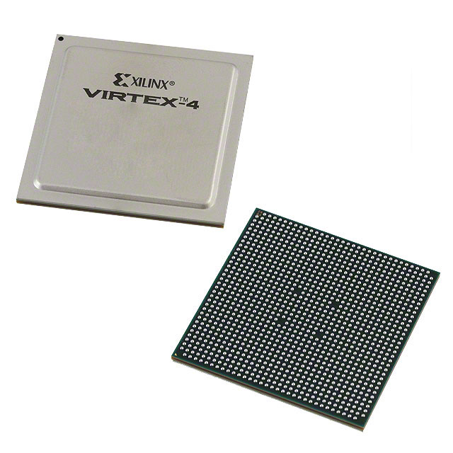
Virtex®-II Pro Field Programmable Gate Array (FPGA) IC 692 3538944 43632 1152-BBGA, FCBGA |
|---|---|
| Quantity | 1,325 Available (as of June 15, 2026) |

| Product Category | Field Programmable Gate Array (FPGA) |
|---|---|
| Manufacturer | AMD |
| Manufacturing Status | Obsolete |
| Manufacturer Standard Lead Time | Contact Us |
| Datasheet |
Specifications & Environmental
| Device Package | 1152-FCBGA (35x35) | Grade | Commercial | Operating Temperature | 0°C – 85°C | ||
|---|---|---|---|---|---|---|---|
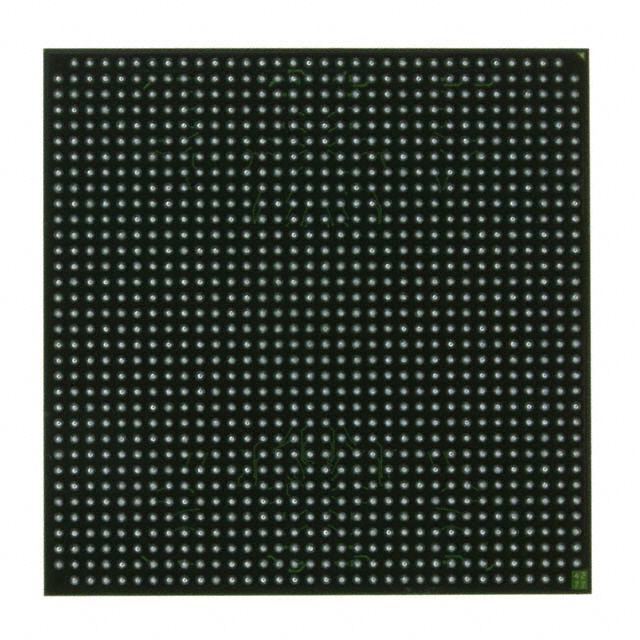
| Package / Case | 1152-BBGA, FCBGA | Number of I/O | 692 | Voltage | 1.425 V - 1.575 V | ||
| Mounting Method | Surface Mount | RoHS Compliance | RoHS non-compliant | REACH Compliance | REACH Unaffected | ||
| Moisture Sensitivity Level | 4 (72 Hours) | Number of LABs/CLBs | 4848 | Number of Logic Elements/Cells | 43632 | ||
| Number of Gates | N/A | ECCN | 3A991D | HTS Code | 8542.39.0001 | ||
| Qualification | N/A | Total RAM Bits | 3538944 |
Overview of XC2VP40-5FF1152C – Virtex®-II Pro Field Programmable Gate Array (1152‑FCBGA)
The XC2VP40-5FF1152C is a Virtex®-II Pro platform FPGA manufactured by AMD. It combines a high logic capacity with substantial embedded memory, a large I/O count and on-chip processor/transceiver resources for applications that require integration of programmable logic, memory and high-speed serial interfaces.
This device targets communications and embedded processing applications where performance, integration and flexible I/O routing matter most. The architecture provides embedded processor block support, multi-gigabit transceiver capability and dedicated DSP resources while operating within a commercial temperature range.
Key Features
- Logic Capacity Approx. 43,632 logic elements suitable for complex control, glue logic and custom datapath implementations.
- Embedded Memory Approximately 3.54 Mbits of on-chip RAM for buffers, FIFOs and local data storage.
- I/O Density 692 I/O pins to support wide parallel interfaces, bus bridging and extensive peripheral connectivity.
- Processor & Transceiver Support Series-level features include support for embedded PowerPC processor blocks and RocketIO/RocketIO X multi-gigabit transceivers for serial link integration.
- DSP Resources Dedicated 18-bit × 18-bit multiplier blocks (series feature) to accelerate arithmetic and signal-processing paths.
- Package & Mounting 1152-FCBGA (35×35) package; surface-mount mounting type for compact board-level integration.
- Power Supply Core supply range: 1.425 V to 1.575 V to match system power-rail requirements.
- Operating Range & Compliance Commercial grade operation from 0 °C to 85 °C; RoHS compliant.
Typical Applications
- Telecom & Datacom Systems Integrate high-speed serial links and protocol bridging using on-chip multi-gigabit transceiver capability and configurable logic.
- Embedded Processing & Control Deploy embedded PowerPC processor blocks alongside programmable logic for system control, protocol processing and real-time tasks.
- Signal Processing & Acceleration Use dedicated multiplier blocks and abundant logic resources for fixed-point DSP, filtering and custom accelerators.
- High-Density I/O Systems Support wide buses and many peripherals with 692 I/O pins for board-level integration and flexible interfacing.
Unique Advantages
- High logic density: Approx. 43,632 logic elements enable complex designs without external glue logic.
- Substantial on-chip memory: Approximately 3.54 Mbits of embedded RAM reduce dependence on external memory for buffering and local storage.
- Large I/O complement: 692 I/Os provide design flexibility for parallel interfaces, buses and mixed-signal front ends.
- Integrated serial and processor capabilities: Series-level support for RocketIO transceivers and PowerPC processor blocks simplifies system integration of serial links and embedded processing.
- Compact FCBGA package: 1152-FCBGA (35×35) package allows dense board integration while maintaining signal routing density.
- Standards-conscious design: RoHS compliance and a clearly specified commercial operating range support predictable manufacturability and deployments in commercial environments.
Why Choose XC2VP40-5FF1152C?
The XC2VP40-5FF1152C positions itself as a highly integrated FPGA choice when designers need a balance of logic capacity, embedded memory and extensive I/O in a single device. Its series-level architectural features—embedded processor blocks, multi-gigabit transceivers and dedicated DSP multipliers—enable consolidated system designs that minimize external components.
This device is well suited for teams developing communications equipment, embedded controllers and DSP-accelerated subsystems that require a mature platform with documented datasheet resources and IP/core references. The combination of on-chip memory, high I/O count and a compact FCBGA package delivers durable value across commercial-grade applications.
Request a quote or submit a purchase enquiry to obtain pricing, availability and lead-time information for XC2VP40-5FF1152C.


Date Founded: 1969
Headquarters: Santa Clara, California, USA
Employees: 25,000+
Revenue: $22.68 Billion
Certifications and Memberships: ISO9001:2015, RoHS, REACH


