
XC2VP40-5FF1152I
| Part Description |
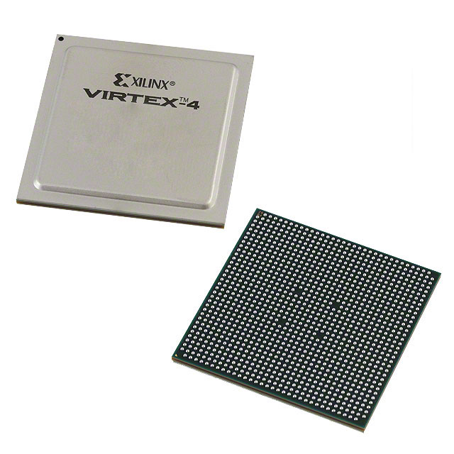
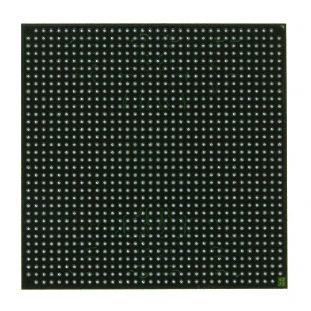
Virtex®-II Pro Field Programmable Gate Array (FPGA) IC 692 3538944 43632 1152-BBGA, FCBGA |
|---|---|
| Quantity | 1,992 Available (as of June 18, 2026) |

| Product Category | Field Programmable Gate Array (FPGA) |
|---|---|
| Manufacturer | AMD |
| Manufacturing Status | Obsolete |
| Manufacturer Standard Lead Time | Contact Us |
| Datasheet |
Specifications & Environmental
| Device Package | 1152-FCBGA (35x35) | Grade | Industrial | Operating Temperature | -40°C – 100°C | ||
|---|---|---|---|---|---|---|---|
| Package / Case | 1152-BBGA, FCBGA | Number of I/O | 692 | Voltage | 1.425 V - 1.575 V | ||
| Mounting Method | Surface Mount | RoHS Compliance | RoHS non-compliant | REACH Compliance | REACH Unaffected | ||
| Moisture Sensitivity Level | 4 (72 Hours) | Number of LABs/CLBs | 4848 | Number of Logic Elements/Cells | 43632 | ||
| Number of Gates | N/A | ECCN | 3A001A7A | HTS Code | 8542.39.0001 | ||
| Qualification | N/A | Total RAM Bits | 3538944 |
Overview of XC2VP40-5FF1152I – Virtex®-II Pro Field Programmable Gate Array (FPGA), 1152-FCBGA
The XC2VP40-5FF1152I is a Virtex®-II Pro platform FPGA in a 1152-ball flip-chip BGA (35×35) package, designed for designs that require high logic density, abundant I/O, and embedded system resources. It integrates a rich FPGA fabric with industry-proven platform features to support high-speed serial interfaces, embedded processing, and on-chip memory.
Targeted at systems-level and industrial applications, this device provides flexible logic resources, multi-megabit embedded RAM, and a large number of I/O to address complex digital processing, communication, and embedded-control tasks.
Key Features
- Logic Fabric 4,848 configurable logic blocks (CLBs) providing approximately 43,632 logic elements for high-density digital design.
- Embedded Memory Approximately 3.54 Mbits of on-chip RAM with 18-Kb Block SelectRAM resources and SelectRAM+ memory hierarchy for buffer and data storage.
- Embedded Multipliers Dedicated 18-bit × 18-bit multiplier blocks for efficient DSP and arithmetic operations.
- High-Speed Serial and Embedded Processing Family-level support for up to twenty RocketIO or RocketIO X multi-gigabit transceivers and up to two IBM PowerPC RISC processor blocks to enable embedded processing and high-speed serial links.
- Clock and I/O Management Integrated digital clock management and SelectI/O™-Ultra technology plus XCITE digitally controlled impedance (DCI) I/O features for robust timing and signal integrity options.
- I/O Density 692 user I/Os to accommodate wide parallel interfaces, peripheral connections, and complex board-level routing.
- Package 1152-ball flip-chip BGA (1152-FCBGA, 35×35) providing a compact, high-pin-count footprint for system integration.
- Power and Temperature Supply voltage range 1.425 V to 1.575 V and industrial operating temperature range of −40°C to 100°C.
- Compliance RoHS compliant.
Typical Applications
- Telecom & Datacom systems Leverages the platform’s multi-gigabit transceiver capabilities and clocking features for high-speed serial transport and protocol implementations.
- Embedded processing platforms Uses the integrated PowerPC processor blocks alongside the FPGA fabric for hardware/software partitioning in control and signal-processing applications.
- High-density logic and DSP Combines abundant CLBs, on-chip RAM, and 18×18 multipliers to implement complex DSP pipelines, packet processing, and custom silicon acceleration.
- Industrial control and automation Industrial-grade temperature range and extensive I/O support system-level interfaces, sensor aggregation, and real-time control functions.
Unique Advantages
- High logic and memory integration: Combines thousands of CLBs with multiple megabits of embedded RAM to reduce external memory footprint and simplify board design.
- Integrated serial and processor resources: On-chip transceivers and PowerPC cores enable tighter system integration and lower BOM for embedded and communication subsystems.
- Robust I/O capacity: 692 I/Os accommodate diverse peripheral and bus interfaces without complex multiplexing or external I/O expanders.
- Industrial operating range: −40°C to 100°C rating supports deployment in demanding environments where temperature resilience is required.
- Compact, high-pin-count package: The 1152-FCBGA (35×35) package delivers high connectivity in a space-efficient footprint for dense PCB layouts.
- Standards-aware feature set: Platform-level features such as RocketIO transceivers, SelectI/O-Ultra, DCMs, and DCI support system designs that require controlled signaling and advanced timing.
Why Choose XC2VP40-5FF1152I?
The XC2VP40-5FF1152I delivers a balanced combination of high logic density, substantial embedded memory, extensive I/O, and platform features that address embedded processing and high-speed serial requirements. Its industrial temperature rating and RoHS compliance make it suitable for performance-driven applications that require reliability and regulatory conformity.
Choose this device when your design demands integrated processing blocks, multi-megabit on-chip RAM, large I/O counts, and platform-level transceiver and I/O capability—helping reduce external components and simplify system architecture while maintaining a compact board footprint.
Request a quote or submit a purchase inquiry to begin procurement for the XC2VP40-5FF1152I. Provide your quantity and delivery requirements to receive pricing and availability information.


Date Founded: 1969
Headquarters: Santa Clara, California, USA
Employees: 25,000+
Revenue: $22.68 Billion
Certifications and Memberships: ISO9001:2015, RoHS, REACH


