
XC2VP40-5FFG1152I
| Part Description |
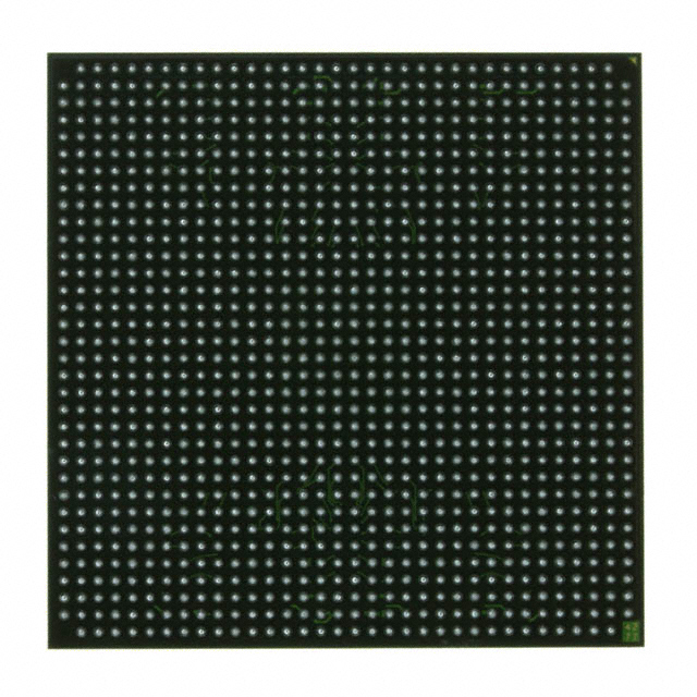
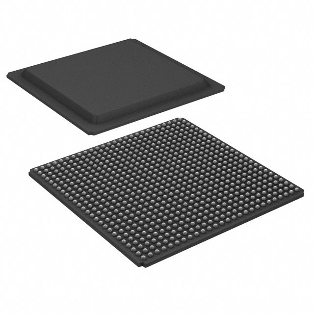
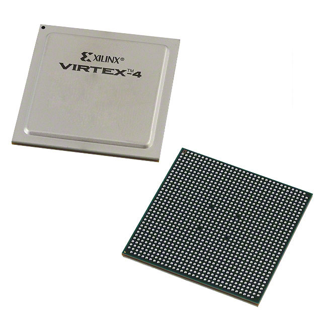
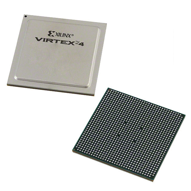
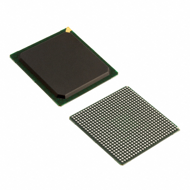
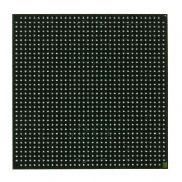
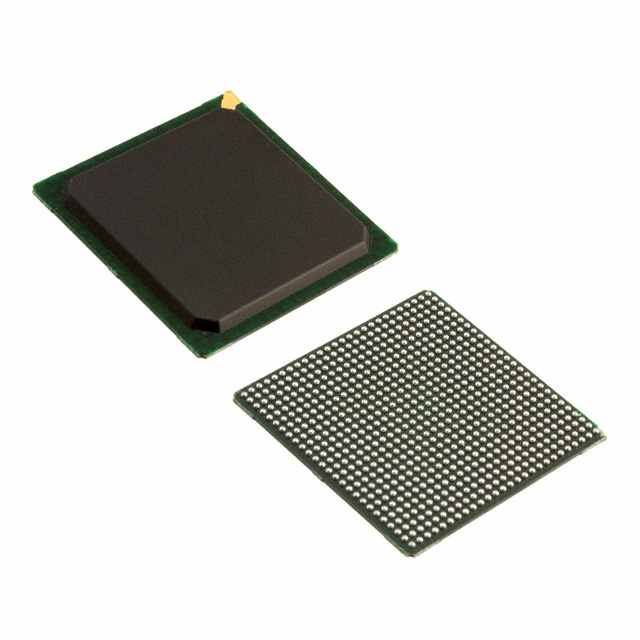
Virtex®-II Pro Field Programmable Gate Array (FPGA) IC 692 3538944 43632 1152-BBGA, FCBGA |
|---|---|
| Quantity | 1,052 Available (as of October 8, 2026) |
| Product Category | Field Programmable Gate Array (FPGA) |
|---|---|
| Manufacturer | AMD |
| Manufacturing Status | Obsolete |
| Manufacturer Standard Lead Time | Contact Us |
| Datasheet |
Specifications & Environmental
| Device Package | 1152-FCBGA (35x35) | Grade | Industrial | Operating Temperature | -40°C – 100°C | ||
|---|---|---|---|---|---|---|---|
| Package / Case | 1152-BBGA, FCBGA | Number of I/O | 692 | Voltage | 1.425 V - 1.575 V | ||
| Mounting Method | Surface Mount | RoHS Compliance | ROHS3 Compliant | REACH Compliance | REACH Unaffected | ||
| Moisture Sensitivity Level | 4 (72 Hours) | Number of LABs/CLBs | 4848 | Number of Logic Elements/Cells | 43632 | ||
| Number of Gates | N/A | ECCN | 3A001A7A | HTS Code | 8542.39.0001 | ||
| Qualification | N/A | Total RAM Bits | 3538944 |
Overview of XC2VP40-5FFG1152I – Virtex®-II Pro Field Programmable Gate Array (FPGA), 1152-FCBGA (Industrial)
The XC2VP40-5FFG1152I is a Virtex®-II Pro family FPGA in a 1152-ball FCBGA package designed for high-density, system-level integration. The device combines a large array of configurable logic, substantial embedded RAM, and a wide complement of I/O to support embedded processing and high-performance digital systems.
Targeted at industrial-grade applications, this surface-mount FPGA delivers a balance of logic capacity, on-chip memory and extensive I/O while operating across a broad industrial temperature range and a tightly specified core voltage.
Key Features
- Logic Capacity — 4,848 CLBs providing 43,632 logic cells for large, complex designs.
- Embedded Memory — Approximately 3.54 Mbits of on-chip RAM (3,538,944 bits) for buffering, FIFOs and local storage.
- I/O Density — 692 user I/O pins to support broad system interfacing and parallel connections.
- Virtex-II Pro Family Capabilities — Family-level features include up to twenty RocketIO or RocketIO X multi-gigabit transceivers and up to two IBM PowerPC RISC processor blocks, plus SelectRAM+ memory hierarchy and dedicated 18×18 multipliers as described in the Virtex-II Pro product specification.
- I/O Technology — Includes SelectI/O™-Ultra and Digitally Controlled Impedance (DCI) I/O functionality in the Virtex-II Pro family for advanced signal integrity and interface options.
- Clock and DSP Support — On-chip clock management circuitry and dedicated multiplier blocks (18-bit × 18-bit) to support DSP and timing-critical functions (family-level feature).
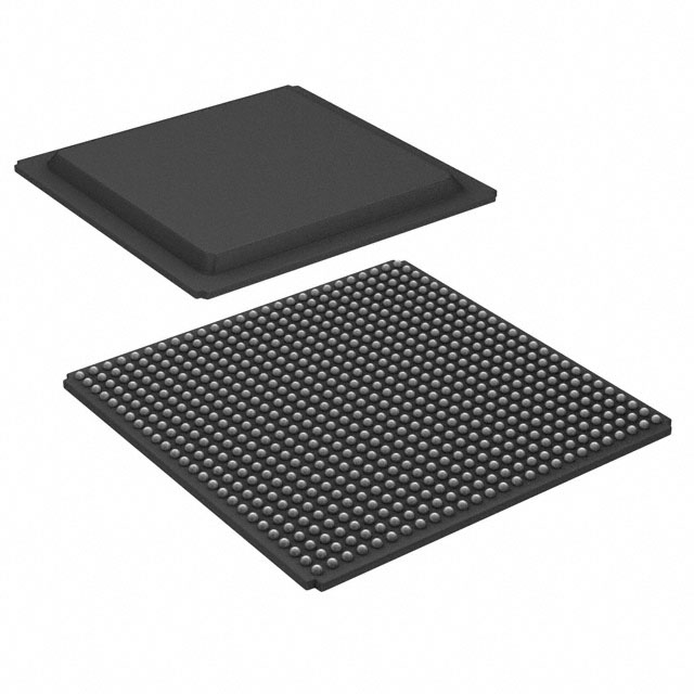
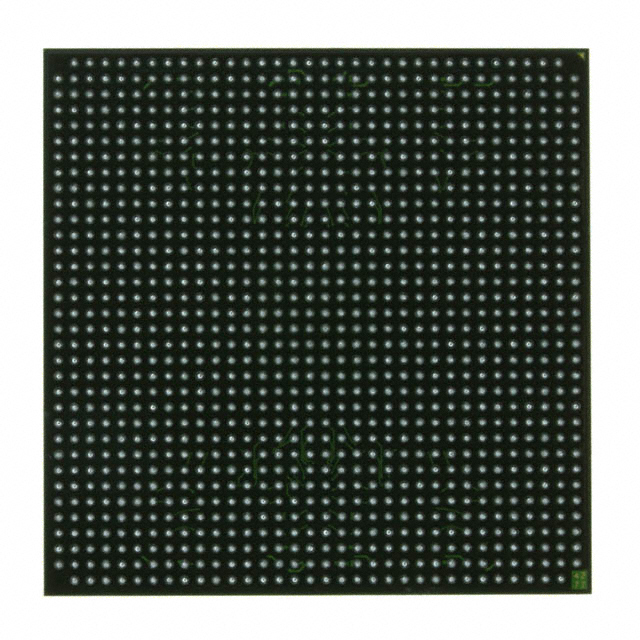
- Package and Mounting — 1152-ball FCBGA (35 × 35 mm) surface-mount package for high-density board integration.
- Power and Voltage — Core voltage supply range 1.425 V to 1.575 V for precise power planning.
- Industrial Temperature Rating — Specified to operate from −40 °C to 100 °C for industrial environments.
- Regulatory Status — RoHS compliant.
Typical Applications
- High-performance embedded systems — Use the dense logic and embedded memory to implement system controllers, protocol bridges, and embedded processing tasks.
- Multi-gigabit communications — Leverage Virtex-II Pro family transceiver and I/O capability for networking and serial link applications that require high channel counts.
- DSP and signal processing — Dedicated 18×18 multipliers and on-chip RAM support filters, FFTs, and other real-time signal-processing pipelines.
- Industrial control and automation — Industrial temperature rating and extensive I/O suit process control, motion control and machine automation systems.
Unique Advantages
- High logic density: 4,848 CLBs and 43,632 logic cells enable substantial on-chip functionality and complex state machines without external ASICs.
- Substantial embedded memory: Approximately 3.54 Mbits of on-chip RAM provides local storage for buffering, queuing and scratchpad needs.
- Extensive I/O: 692 user I/O pins allow flexible system interfacing and high parallel throughput for data acquisition and control.
- Industrial-ready thermal range: Specified −40 °C to 100 °C operation supports deployment in demanding environments.
- Precision supply window: Core voltage 1.425 V–1.575 V enables predictable power budgeting and compatibility with target systems that adhere to that supply domain.
- Mature platform features: Virtex-II Pro family architecture offers embedded processor blocks, advanced transceivers and clock-management resources for system-level integration.
Why Choose XC2VP40-5FFG1152I?
The XC2VP40-5FFG1152I presents a compelling option when you need a high-density FPGA with ample on-chip memory, broad I/O, and industrial temperature capability. Its 1152-ball FCBGA package and compact core voltage range make it suitable for compact, power-sensitive system boards while providing the resources required for complex logic, DSP and embedded processing tasks.
This device is well suited to engineering teams building industrial controls, communications endpoints, or high-throughput digital subsystems that require a combination of integration, configurability and field-proven family features.
Request a quote or submit a parts inquiry to get pricing and availability for the XC2VP40-5FFG1152I.





















Date Founded: 1969
Headquarters: Santa Clara, California, USA
Employees: 25,000+
Revenue: $22.68 Billion
Certifications and Memberships: ISO9001:2015, RoHS, REACH











