
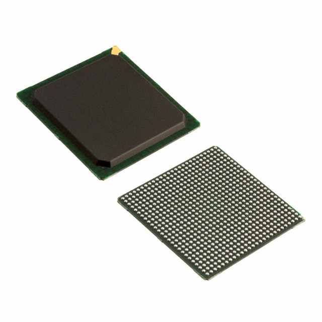
XC2VP40-5FGG676C
| Part Description |
Virtex®-II Pro Field Programmable Gate Array (FPGA) IC 416 3538944 43632 676-BGA |
|---|---|
| Quantity | 1,781 Available (as of June 15, 2026) |
| Product Category | Field Programmable Gate Array (FPGA) |
|---|---|
| Manufacturer | AMD |
| Manufacturing Status | Obsolete |
| Manufacturer Standard Lead Time | Contact Us |
| Datasheet |
Specifications & Environmental
| Device Package | 676-FBGA (27x27) | Grade | Commercial | Operating Temperature | 0°C – 85°C | ||
|---|---|---|---|---|---|---|---|
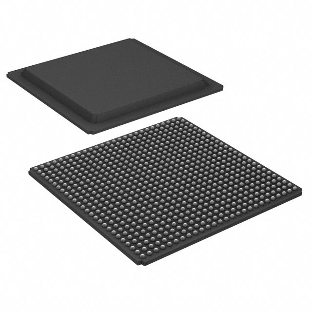
| Package / Case | 676-BGA | Number of I/O | 416 | Voltage | 1.425 V - 1.575 V | ||
| Mounting Method | Surface Mount | RoHS Compliance | RoHS non-compliant | REACH Compliance | REACH Unaffected | ||
| Moisture Sensitivity Level | 3 (168 Hours) | Number of LABs/CLBs | 4848 | Number of Logic Elements/Cells | 43632 | ||
| Number of Gates | N/A | ECCN | 3A001A7A | HTS Code | 8542.39.0001 | ||
| Qualification | N/A | Total RAM Bits | 3538944 |
Overview of XC2VP40-5FGG676C – Virtex®-II Pro FPGA, 676-BGA
The XC2VP40-5FGG676C is a Virtex®-II Pro platform Field Programmable Gate Array (FPGA) supplied in a 676-ball fine-pitch BGA package. It combines a large logic fabric with embedded memory and a high pin count to address demanding embedded and communications-oriented designs.
Designed for applications that require extensive logic resources, embedded RAM, and robust I/O capability, this device delivers the architecture and system-level features associated with the Virtex-II Pro family.
Key Features
- Logic Capacity — 4,848 CLBs (configurable logic blocks) providing 43,632 logic elements for complex logic and control functions.
- Embedded Memory — Approximately 3.54 Mbits of on-chip RAM (3,538,944 total RAM bits) for frame buffering, packet processing, and local storage.
- Dedicated DSP Resources — Family-level support for 18-bit × 18-bit multiplier blocks for high-throughput arithmetic and signal-processing kernels.
- I/O Density — Up to 416 user I/O pins to interface with high-pin-count peripherals, memory buses, and board-level interfaces.
- Power & Supply — Core voltage supply range of 1.425 V to 1.575 V to match system power rails and design margins.
- Package & Mounting — 676-ball FBGA (27 × 27) surface-mount package for dense board integration and reliable soldering.
- Operating Range — Commercial grade operation from 0 °C to 85 °C for standard temperature environments.
- RoHS Compliance — Device is RoHS compliant.
- Virtex-II Pro Family Capabilities — Family-level features include support for embedded processor blocks (PowerPC™), RocketIO multi-gigabit transceiver technology, digitally controlled impedance (DCI), SelectI/O™-Ultra options, and on-chip clock management (as described in the Virtex-II Pro product specification).
Typical Applications
- Telecommunications & Datacom — Use the family’s RocketIO transceiver capabilities and high I/O count for line cards, protocol processing, and high-speed serial links.
- Embedded Processing — Leverage the Virtex-II Pro platform’s embedded processor block support for system-on-chip designs and real-time control tasks.
- Signal Processing — Employ dedicated multiplier blocks and abundant on-chip RAM for filters, FFTs, and other DSP pipelines.
- Prototype and Development Platforms — High logic capacity and I/O density make this device suitable for complex prototype boards and hardware validation platforms.
Unique Advantages
- High Logic Density: 43,632 logic elements and 4,848 CLBs enable integration of complex control, protocol, and data-path logic within a single device.
- Substantial Embedded Memory: Approximately 3.54 Mbits of on-chip RAM reduces external memory dependence and accelerates data buffering and local processing.
- Extensive I/O Connectivity: 416 I/O pins support broad interfacing options for high-speed buses, peripherals, and multi-board systems.
- Platform-Level Integration: Virtex-II Pro family features such as embedded processor blocks, RocketIO transceivers, and SelectI/O support simplify system-level design and IP reuse.
- Standard Commercial Range: Commercial operating temperature and surface-mount FBGA packaging simplify deployment in mainstream embedded and communications equipment.
- Regulatory Compliance: RoHS compliance supports environmentally conscious manufacturing and supply-chain requirements.
Why Choose XC2VP40-5FGG676C?
The XC2VP40-5FGG676C places a large Virtex-II Pro FPGA fabric, substantial embedded memory, and high I/O density into a compact 676-ball FBGA package. It is well suited for designers building complex embedded systems, communications modules, and signal-processing applications that require integrated logic, memory, and robust interfacing.
Backed by the Virtex-II Pro platform’s family-level architecture and IP support, the device is appropriate for teams that need scalable FPGA capacity paired with embedded-processing and high-speed I/O options. Its commercial temperature rating and RoHS compliance align it with standard production and development environments.
Request a quote or submit your requirements to receive pricing and availability for the XC2VP40-5FGG676C. Our team will respond with a tailored quotation and lead-time information.


Date Founded: 1969
Headquarters: Santa Clara, California, USA
Employees: 25,000+
Revenue: $22.68 Billion
Certifications and Memberships: ISO9001:2015, RoHS, REACH


