
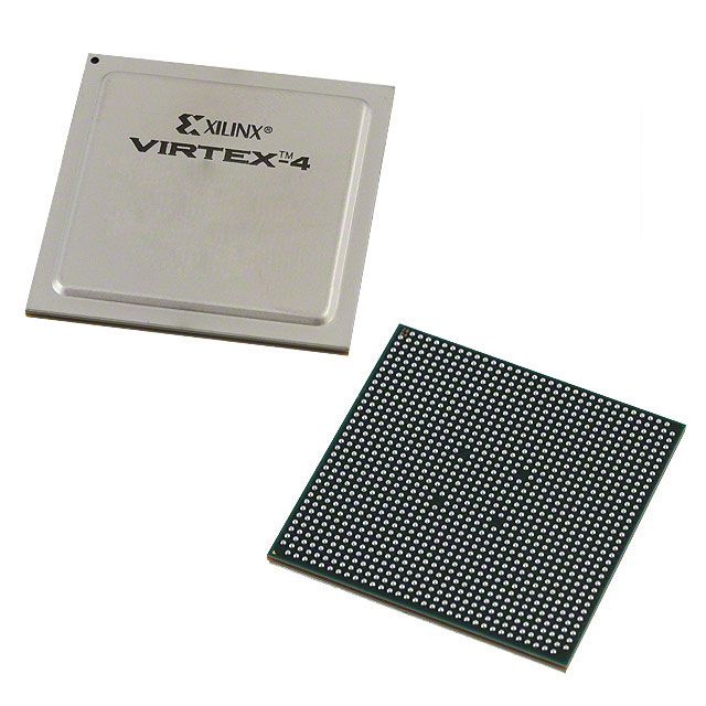
XC2VP40-6FF1148C
| Part Description |
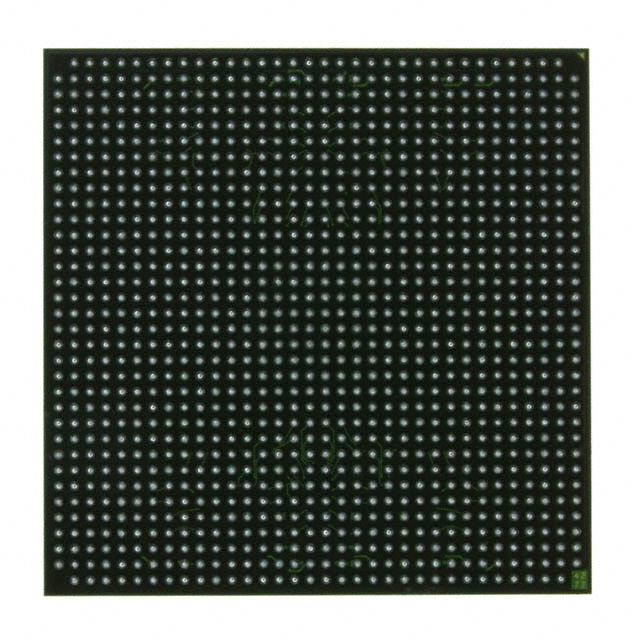
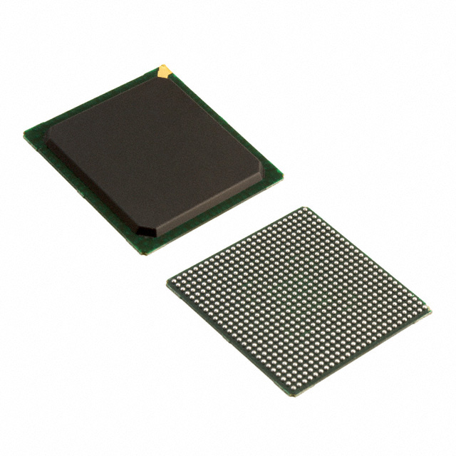
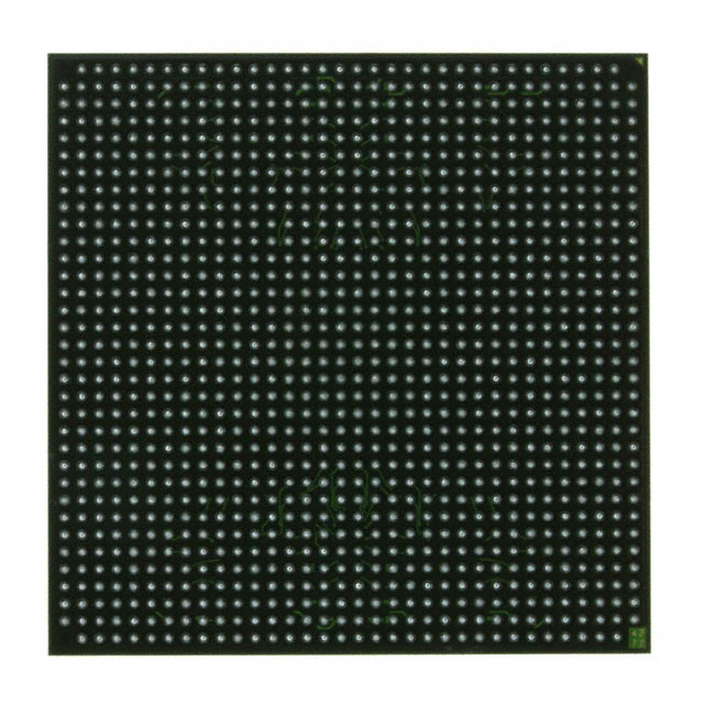
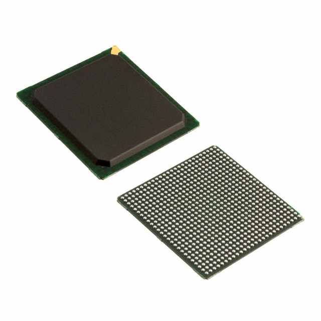
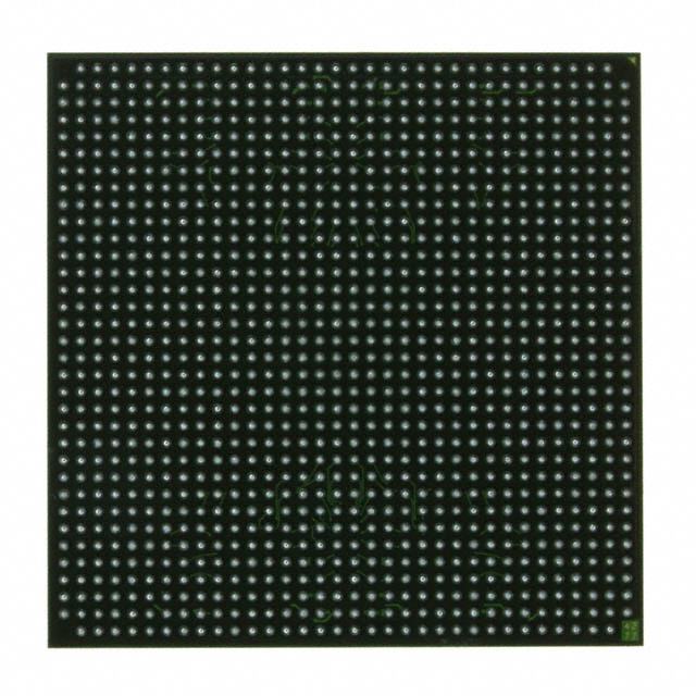
Virtex®-II Pro Field Programmable Gate Array (FPGA) IC 804 3538944 43632 1148-BBGA, FCBGA |
|---|---|
| Quantity | 121 Available (as of October 8, 2026) |
| Product Category | Field Programmable Gate Array (FPGA) |
|---|---|
| Manufacturer | AMD |
| Manufacturing Status | Obsolete |
| Manufacturer Standard Lead Time | Contact Us |
| Datasheet |
Specifications & Environmental
| Device Package | 1148-FCPBGA (35x35) | Grade | Commercial | Operating Temperature | 0°C – 85°C | ||
|---|---|---|---|---|---|---|---|
| Package / Case | 1148-BBGA, FCBGA | Number of I/O | 804 | Voltage | 1.425 V - 1.575 V | ||
| Mounting Method | Surface Mount | RoHS Compliance | RoHS non-compliant | REACH Compliance | REACH Unaffected | ||
| Moisture Sensitivity Level | 4 (72 Hours) | Number of LABs/CLBs | 4848 | Number of Logic Elements/Cells | 43632 | ||
| Number of Gates | N/A | ECCN | 3A001A7A | HTS Code | 8542.39.0001 | ||
| Qualification | N/A | Total RAM Bits | 3538944 |
Overview of XC2VP40-6FF1148C – Virtex‑II Pro FPGA, 1148‑BBGA (FCBGA)
The XC2VP40-6FF1148C is a Virtex‑II Pro field‑programmable gate array (FPGA) in an 1148‑ball flip‑chip BGA (FCBGA) package, supplied by AMD. It combines high-density logic, embedded memory, and extensive I/O to support complex digital designs.
As a member of the Virtex‑II Pro family, the device supports embedded processor blocks and multi‑gigabit transceiver technology at the family level and is suited to applications that require integrated processing, large I/O counts, and substantial on‑chip RAM and DSP resources.
Key Features
- Logic Resources 43,632 logic elements and 4,848 CLB resources provide high-density programmable logic for complex system functions.
- Embedded Memory Approximately 3.54 Mbits of on‑chip RAM (3,538,944 total RAM bits) for buffering, packet storage, and intermediate data.
- I/O Capacity Up to 804 user I/O pins enable broad external connectivity and high channel counts for multi‑lane interfaces.
- Processor & Transceiver Support Virtex‑II Pro family features include up to two embedded PowerPC processor blocks and support for RocketIO/RocketIO X multi‑gigabit transceivers, enabling integrated processor and high‑speed serial interface options.
- DSP Resources Dedicated 18‑bit × 18‑bit multiplier blocks, providing hardware acceleration for arithmetic and signal processing tasks (family feature).
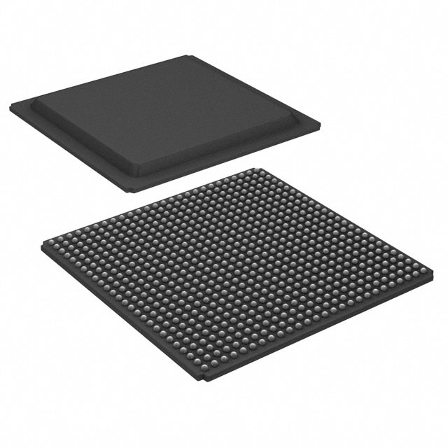
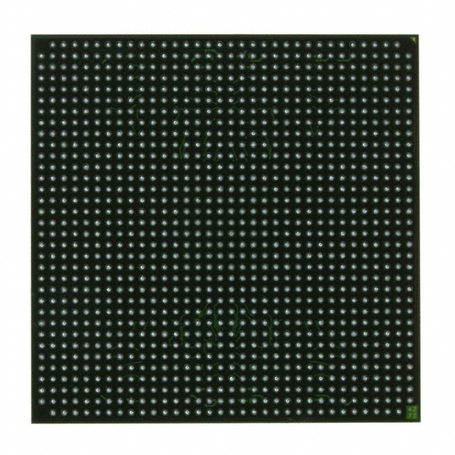
- Package & Mounting 1148‑BBGA (FCBGA) package in a 35 × 35 mm footprint with surface‑mount assembly for compact, high‑density board designs.
- Power Nominal core supply range of 1.425 V to 1.575 V for regulated core power design.
- Operating Conditions Commercial grade with an operating temperature range of 0 °C to 85 °C.
- Environmental Compliance RoHS compliant for lead‑free manufacturing processes.
Typical Applications
- Telecommunications & Data Communications Family‑level RocketIO transceiver support and high I/O counts make the device suitable for serial link aggregation, backplane interfaces, and protocol bridging.
- Embedded Processing & Control Integrated processor block support combined with abundant logic elements and memory enables system control, protocol handling, and embedded application offload.
- Signal Processing & Acceleration On‑chip RAM and 18×18 multipliers provide resources for filtering, DSP acceleration, and real‑time data processing.
- High‑density System Integration Large logic capacity and 804 I/Os support consolidating multiple functions into a single FPGA for compact, integrated system designs.
Unique Advantages
- Highly integrated logic and memory: 43,632 logic elements and approximately 3.54 Mbits of embedded RAM reduce external component needs and simplify board architecture.
- Extensive I/O headroom: 804 I/Os enable wide parallel interfaces and many serial lanes without additional bridge devices.
- Embedded processing capability: Family support for PowerPC processor blocks lets designers integrate control and data‑plane functions on a single device.
- Built for high‑speed serial links: Virtex‑II Pro family RocketIO transceivers and telecom/datacom support modes provide options for multi‑gigabit serial connectivity.
- Compact, manufacturable package: 1148‑BBGA (FCBGA) 35×35 mm surface‑mount package supports dense board layouts and standard SMT assembly.
- Regulatory readiness: RoHS compliance aligns with lead‑free manufacturing requirements.
Why Choose XC2VP40-6FF1148C?
The XC2VP40-6FF1148C places substantial programmable logic, embedded RAM, and high I/O capacity into a compact FCBGA footprint, making it a strong option for designs that require integrated processing, significant on‑chip memory, and broad external interfacing. Its Virtex‑II Pro family features—such as dedicated multipliers, processor block support, and multi‑gigabit transceiver capability at the family level—help consolidate system functions and reduce board complexity.
This device is positioned for engineering teams building commercial‑grade systems that need scalable logic density, ample I/O, and the architectural options provided by the Virtex‑II Pro platform. The combination of quantifiable resources and family‑level features supports long‑term designs where integration and performance are key considerations.
Request a quote or submit an inquiry to purchase the XC2VP40-6FF1148C and discuss availability and lead times with our team.





















Date Founded: 1969
Headquarters: Santa Clara, California, USA
Employees: 25,000+
Revenue: $22.68 Billion
Certifications and Memberships: ISO9001:2015, RoHS, REACH











