
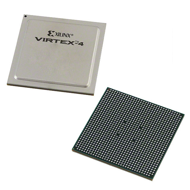
XC2VP40-5FG676I
| Part Description |
Virtex®-II Pro Field Programmable Gate Array (FPGA) IC 416 3538944 43632 676-BGA |
|---|---|
| Quantity | 234 Available (as of June 10, 2026) |

| Product Category | Field Programmable Gate Array (FPGA) |
|---|---|
| Manufacturer | AMD |
| Manufacturing Status | Obsolete |
| Manufacturer Standard Lead Time | Contact Us |
| Datasheet |
Specifications & Environmental
| Device Package | 676-FBGA (27x27) | Grade | Industrial | Operating Temperature | -40°C – 100°C | ||
|---|---|---|---|---|---|---|---|
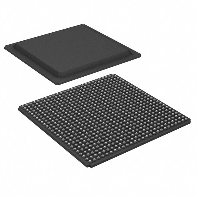
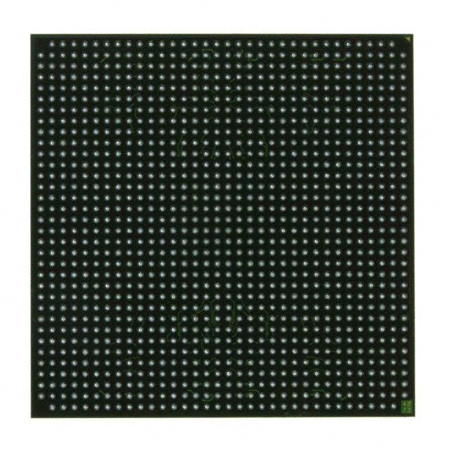
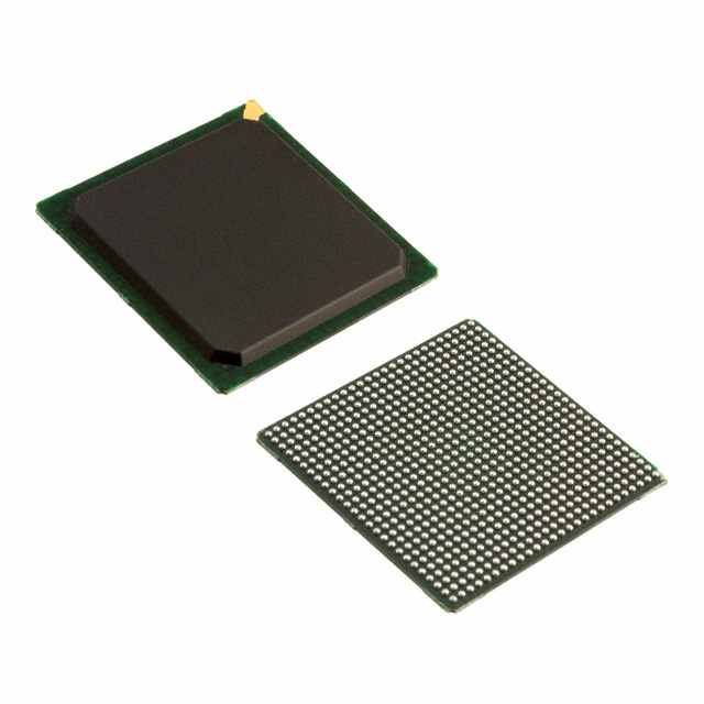
| Package / Case | 676-BGA | Number of I/O | 416 | Voltage | 1.425 V - 1.575 V | ||
| Mounting Method | Surface Mount | RoHS Compliance | RoHS non-compliant | REACH Compliance | REACH Unaffected | ||
| Moisture Sensitivity Level | 3 (168 Hours) | Number of LABs/CLBs | 4848 | Number of Logic Elements/Cells | 43632 | ||
| Number of Gates | N/A | ECCN | 3A001A7A | HTS Code | 8542.39.0001 | ||
| Qualification | N/A | Total RAM Bits | 3538944 |
Overview of XC2VP40-5FG676I – Virtex®-II Pro FPGA, 676‑BGA, Industrial
The XC2VP40-5FG676I is a Virtex®-II Pro field programmable gate array (FPGA) offered in a 676‑BGA surface‑mount package. It delivers a combination of programmable logic, on‑chip embedded memory, and extensive I/O for system designs requiring high logic capacity and flexible integration.
Key on‑device specifications include approximately 43,632 logic elements, approximately 3.54 Mbits of embedded memory, 416 user I/Os, a 1.425–1.575 V core supply range, and an industrial operating temperature range of −40 °C to 100 °C. Family documentation for Virtex‑II Pro devices also details integrated features such as RocketIO multi‑gigabit transceivers, embedded PowerPC processor blocks, dedicated multipliers, and advanced clocking resources.
Key Features
- Core & architecture Virtex‑II Pro FPGA platform architecture with family‑level support for embedded PowerPC™ processor blocks and integrated multi‑gigabit transceivers (RocketIO/RocketIO X).
- Logic capacity Approximately 43,632 logic elements for implementing complex digital functions and control logic.
- Embedded memory Approximately 3.54 Mbits (3,538,944 bits) of on‑chip RAM for buffering, FIFOs, and memory‑centric logic.
- I/O & serial interfaces 416 user I/O pins; family documentation includes support for RocketIO multi‑gigabit transceivers for high‑bandwidth serial links.
- Arithmetic and DSP resources Family features include dedicated 18‑bit × 18‑bit multiplier blocks suitable for DSP kernels and arithmetic acceleration.
- Clocking and timing Integrated clock management resources such as Digital Clock Manager (DCM) and global clocking for synchronous system designs (family feature).
- I/O technology SelectI/O™ and Digitally Controlled Impedance (DCI) family features for flexible interfacing and signal integrity management.
- Package and mounting 676‑BGA (supplier package 676‑FBGA, 27 × 27) in a surface‑mount form factor for dense board integration.
- Electrical and environmental Core supply voltage 1.425–1.575 V; operating temperature −40 °C to 100 °C; RoHS compliant.
Typical Applications
- High‑speed communications Multi‑gigabit transceiver support and abundant I/O make this device suitable for serial links, backplane interfaces, and data transport modules.
- Embedded processing and control Family support for embedded PowerPC processor blocks plus large logic and memory resources supports system control, protocol handling, and embedded software acceleration.
- DSP and signal processing Dedicated multiplier blocks and on‑chip RAM enable implementation of filtering, transforms, and other real‑time signal processing functions.
- Complex system integration High logic density and 416 I/Os allow consolidation of multiple functions into a single FPGA for board‑level integration and BOM reduction.
Unique Advantages
- Significant logic density: Approximately 43,632 logic elements let you implement complex state machines, datapaths, and control logic without excessive partitioning.
- Substantial on‑chip memory: Approximately 3.54 Mbits of embedded RAM reduces dependence on external memory for buffers and local storage.
- High‑density I/O and packaging: 416 user I/Os in a 676‑BGA package support dense board routing and multiple peripheral interfaces.
- Family support for high‑speed serial links: RocketIO transceivers (family feature) provide a pathway to multi‑gigabit connectivity for networked and telecom applications.
- Industrial temperature and RoHS compliance: −40 °C to 100 °C operating range and RoHS status align with industrial deployment requirements.
Why Choose XC2VP40-5FG676I?
The XC2VP40-5FG676I places substantial programmable logic, embedded memory, and dense I/O into a single 676‑BGA surface‑mount package, suited for designs that require integration of complex logic, on‑chip buffering, and multiple interfaces. Its industrial temperature rating and RoHS compliance make it applicable across a wide range of board‑level systems.
Supported by comprehensive Virtex‑II Pro family documentation, the device is appropriate for engineers developing high‑performance communications, embedded processing, and DSP‑intensive applications that benefit from on‑chip multipliers, clock management, and available multi‑gigabit transceiver technology.
Request a quote or submit an inquiry to check pricing and availability for the XC2VP40-5FG676I. Our team can provide technical and procurement details to support your design cycle.


Date Founded: 1969
Headquarters: Santa Clara, California, USA
Employees: 25,000+
Revenue: $22.68 Billion
Certifications and Memberships: ISO9001:2015, RoHS, REACH


