
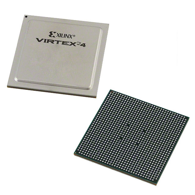
XC2VP40-5FFG1152C
| Part Description |
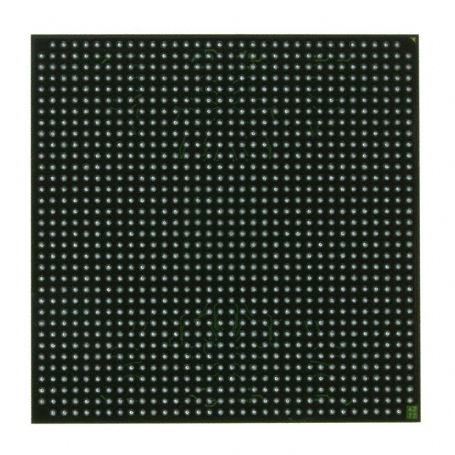
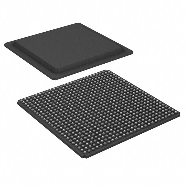
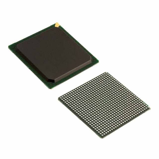
Virtex®-II Pro Field Programmable Gate Array (FPGA) IC 692 3538944 43632 1152-BBGA, FCBGA |
|---|---|
| Quantity | 1,626 Available (as of June 18, 2026) |
| Product Category | Field Programmable Gate Array (FPGA) |
|---|---|
| Manufacturer | AMD |
| Manufacturing Status | Obsolete |
| Manufacturer Standard Lead Time | Contact Us |
| Datasheet |
Specifications & Environmental
| Device Package | 1152-FCBGA (35x35) | Grade | Commercial | Operating Temperature | 0°C – 85°C | ||
|---|---|---|---|---|---|---|---|
| Package / Case | 1152-BBGA, FCBGA | Number of I/O | 692 | Voltage | 1.425 V - 1.575 V | ||
| Mounting Method | Surface Mount | RoHS Compliance | RoHS non-compliant | REACH Compliance | REACH Unaffected | ||
| Moisture Sensitivity Level | 4 (72 Hours) | Number of LABs/CLBs | 4848 | Number of Logic Elements/Cells | 43632 | ||
| Number of Gates | N/A | ECCN | 3A001A7A | HTS Code | 8542.39.0001 | ||
| Qualification | N/A | Total RAM Bits | 3538944 |
Overview of XC2VP40-5FFG1152C – Virtex®-II Pro FPGA, 43,632 Logic Elements, 1152‑FCBGA
The XC2VP40-5FFG1152C is a Virtex®-II Pro family Field Programmable Gate Array packaged in a 1152‑ball FCBGA (35×35) designed for commercial embedded and communications applications. The device combines a high logic element count, substantial on‑chip RAM, and a large I/O complement to address complex digital signal processing, embedded processing, and high‑density I/O tasks.
Key Features
- Logic Capacity 4,848 CLBs providing 43,632 logic elements for implementing complex digital functions and system logic.
- Embedded Memory Approximately 3.54 Mbits of total on‑chip RAM to support frame buffering, FIFOs, and intermediate storage for DSP and control tasks.
- I/O Density 692 user I/O pins enable wide parallel interfaces, dense board routing, and flexible external connectivity options.
- Power Supply Core voltage range of 1.425 V to 1.575 V for consistent integration with standard FPGA power architectures.
- Package & Mounting 1152‑BBGA (1152‑FCBGA, 35×35) surface‑mount package optimized for high I/O count and compact board footprint.
- Operating Range & Grade Commercial grade with an operating temperature range of 0 °C to 85 °C suitable for standard commercial embedded systems.
- Standards & Compliance RoHS compliant for reduced hazardous substance requirements in commercial electronics.
- Virtex‑II Pro Platform Features (family‑level) The Virtex‑II Pro platform includes architecture elements such as configurable logic blocks, dedicated 18×18 multipliers, SelectRAM memory hierarchy, and family support for embedded processor blocks and multi‑gigabit transceivers (family documentation provides further details).
Typical Applications
- Telecom & Datacom Systems Family‑level support for multi‑gigabit transceiver functionality and high I/O count make the device suitable for line cards, protocol processing, and packet buffering.
- Embedded Processing & Control Large logic capacity and substantial embedded RAM enable implementation of embedded control, custom accelerators, and system glue logic.
- High‑Density Prototyping & FPGA‑based Systems The combination of CLB density and extensive I/O supports complex prototypes and board‑level implementations requiring many external connections.
Unique Advantages
- High Logic Density: 43,632 logic elements enable integration of multiple subsystems and large RTL designs on a single device.
- Significant On‑Chip Memory: Approximately 3.54 Mbits of RAM reduces dependence on external memory for buffering and data paths.
- Extensive I/O Count: 692 I/O pins provide the flexibility to interface with wide buses, high‑pin connectors, and multiple peripherals without external multiplexing.
- Compact, High‑Pin Package: 1152‑FCBGA (35×35) delivers high I/O density in a compact footprint for efficient board integration.
- Commercial‑Grade Operation: Specified for 0 °C to 85 °C operation to meet standard commercial deployment requirements.
- RoHS Compliant: Aligns with common environmental and manufacturing requirements for commercial electronics.
Why Choose XC2VP40-5FFG1152C?
The XC2VP40-5FFG1152C positions itself as a capable Virtex®‑II Pro family FPGA for engineers requiring substantial logic, embedded memory, and high I/O density in a commercial surface‑mount package. Its combination of CLBs, logic elements, and on‑chip RAM delivers the resources needed for complex embedded designs, protocol processing, and FPGA‑based system integration.
Backed by the Virtex‑II Pro platform documentation and family resources, this device is suited to teams building high‑performance prototypes and production systems that rely on flexible, reprogrammable logic and rich I/O in a 1152‑ball FCBGA footprint.
Request a quote or submit an inquiry to receive pricing and availability for XC2VP40-5FFG1152C.


Date Founded: 1969
Headquarters: Santa Clara, California, USA
Employees: 25,000+
Revenue: $22.68 Billion
Certifications and Memberships: ISO9001:2015, RoHS, REACH


