
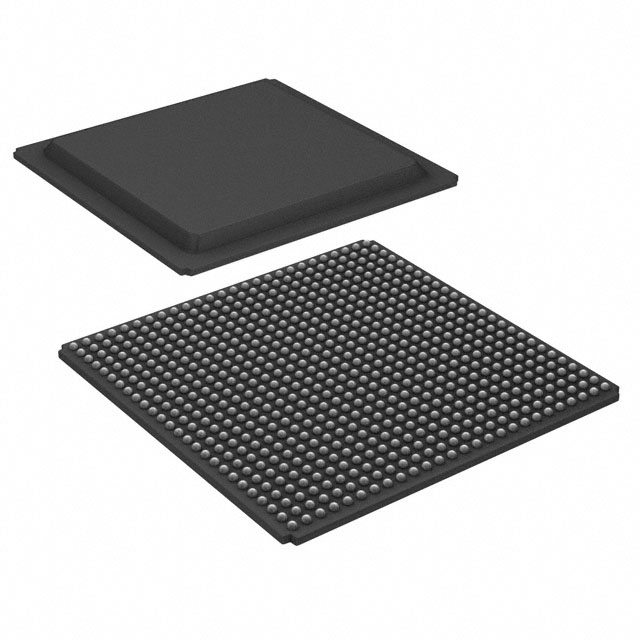
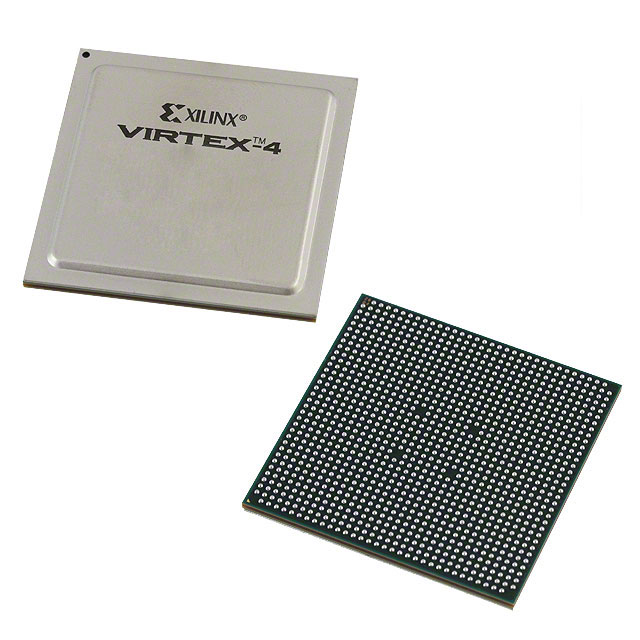
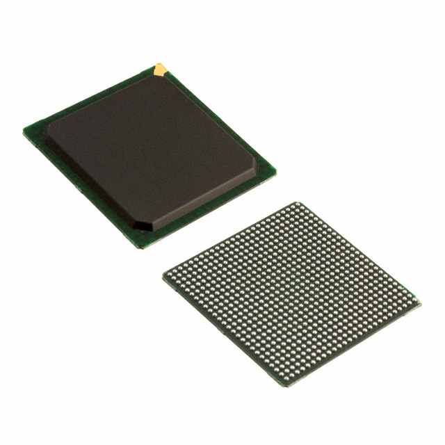
XC2VP40-5FG676C
| Part Description |
Virtex®-II Pro Field Programmable Gate Array (FPGA) IC 416 3538944 43632 676-BGA |
|---|---|
| Quantity | 631 Available (as of June 8, 2026) |
| Product Category | Field Programmable Gate Array (FPGA) |
|---|---|
| Manufacturer | AMD |
| Manufacturing Status | Obsolete |
| Manufacturer Standard Lead Time | Contact Us |
| Datasheet |
Specifications & Environmental
| Device Package | 676-FBGA (27x27) | Grade | Commercial | Operating Temperature | 0°C – 85°C | ||
|---|---|---|---|---|---|---|---|
| Package / Case | 676-BGA | Number of I/O | 416 | Voltage | 1.425 V - 1.575 V | ||
| Mounting Method | Surface Mount | RoHS Compliance | RoHS non-compliant | REACH Compliance | REACH Unaffected | ||
| Moisture Sensitivity Level | 2A (4 Weeks) | Number of LABs/CLBs | 4848 | Number of Logic Elements/Cells | 43632 | ||
| Number of Gates | N/A | ECCN | 3A991D | HTS Code | 8542.39.0001 | ||
| Qualification | N/A | Total RAM Bits | 3538944 |
Overview of XC2VP40-5FG676C – Virtex®-II Pro FPGA, 676-BGA
The XC2VP40-5FG676C is a Virtex®-II Pro field programmable gate array (FPGA) IC supplied in a 676-ball fine-pitch BGA package. It provides a high-density reconfigurable logic platform with substantial on-chip memory, a high I/O count and proven platform features for designs that require flexible logic resources and system-level integration.
Key raw capabilities include 4,848 configurable logic blocks (CLBs) delivering 43,632 logic elements, approximately 3.54 Mbits of embedded memory, and 416 user I/Os. The device is a surface-mount component in a 676-FBGA (27×27) package, operates from a 1.425–1.575 V core supply and is specified for commercial temperature operation (0 °C to 85 °C).
Key Features
- Logic Capacity 4,848 CLBs providing 43,632 logic elements suitable for complex glue logic, protocol implemention and custom datapaths.
- Embedded Memory Approximately 3.54 Mbits of on-chip RAM to support buffering, lookup tables and state storage without external memory.
- I/O Density 416 user I/Os to support wide parallel interfaces, bus connections and mixed-signal front-end routing.
- Power and Supply Core voltage range 1.425 V to 1.575 V for integration into regulated power architectures.
- Package and Mounting 676-ball Fine-Pitch BGA (676-FBGA, 27×27) in a surface-mount form factor for compact, high-density board designs.
- Operating Range & Compliance Commercial grade operation from 0 °C to 85 °C and RoHS-compliant construction.
- Platform-Level Capabilities Virtex-II Pro family features include embedded processor block support and multi-gigabit transceiver architecture (family-level information from the Virtex-II Pro platform specification).
Typical Applications
- Communications & Networking High I/O count and platform transceiver features make the device suitable for protocol bridging, packet processing and interface aggregation in telecom and datacom systems.
- Embedded Processing On-chip memory and family-level processor block support enable offload of control and real-time tasks within embedded systems.
- Prototyping & System Integration Dense logic and large I/O resources support rapid hardware validation and integration of complex digital subsystems.
- Signal Processing Acceleration Dedicated multiplier resources and abundant local RAM make the FPGA appropriate for fixed-function DSP blocks and pipeline acceleration.
Unique Advantages
- High-density logic in a single device: 43,632 logic elements provide significant integration of custom logic without multiple chips.
- Substantial on-chip memory: approximately 3.54 Mbits of embedded RAM reduces external memory dependence and lowers BOM complexity.
- Large I/O footprint: 416 I/Os enable broad interfacing options for parallel buses, connectors and mixed I/O applications.
- Compact package option: 676-FBGA (27×27) provides a small PCB footprint while maintaining high pin count for dense system layouts.
- Commercial-grade qualification: Specified for 0 °C to 85 °C operation and RoHS compliance for mainstream electronics projects.
Why Choose XC2VP40-5FG676C?
The XC2VP40-5FG676C positions itself as a high-capacity Virtex®-II Pro platform FPGA with a blend of logic density, embedded memory and extensive I/O suitable for system designers who need a reconfigurable, integrated solution. Its combination of CLBs, large embedded RAM and high I/O count supports consolidation of multiple functions onto a single device, reducing board complexity and part count.
This device is well suited to engineering teams developing communications equipment, embedded processing platforms, and hardware-accelerated functions where reliable commercial-grade operation and RoHS compliance are required. The Virtex-II Pro family-level architecture provides a foundation of capabilities that can be applied across a range of design requirements.
Request a quote or submit an inquiry for pricing and availability of XC2VP40-5FG676C to get lead-time and order information tailored to your project needs.


Date Founded: 1969
Headquarters: Santa Clara, California, USA
Employees: 25,000+
Revenue: $22.68 Billion
Certifications and Memberships: ISO9001:2015, RoHS, REACH


