
XC2VP40-5FF1148C
| Part Description |
Virtex®-II Pro Field Programmable Gate Array (FPGA) IC 804 3538944 43632 1148-BBGA, FCBGA |
|---|---|
| Quantity | 513 Available (as of June 10, 2026) |

| Product Category | Field Programmable Gate Array (FPGA) |
|---|---|
| Manufacturer | AMD |
| Manufacturing Status | Obsolete |
| Manufacturer Standard Lead Time | Contact Us |
| Datasheet |
Specifications & Environmental
| Device Package | 1148-FCPBGA (35x35) | Grade | Commercial | Operating Temperature | 0°C – 85°C | ||
|---|---|---|---|---|---|---|---|
| Package / Case | 1148-BBGA, FCBGA | Number of I/O | 804 | Voltage | 1.425 V - 1.575 V | ||
| Mounting Method | Surface Mount | RoHS Compliance | RoHS non-compliant | REACH Compliance | REACH Unaffected | ||
| Moisture Sensitivity Level | 4 (72 Hours) | Number of LABs/CLBs | 4848 | Number of Logic Elements/Cells | 43632 | ||
| Number of Gates | N/A | ECCN | 3A001A7A | HTS Code | 8542.39.0001 | ||
| Qualification | N/A | Total RAM Bits | 3538944 |
Overview of XC2VP40-5FF1148C – Virtex®-II Pro FPGA, 1148-BBGA
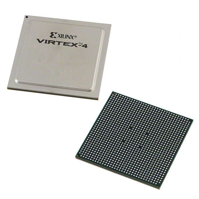
The XC2VP40-5FF1148C is a Virtex®-II Pro field programmable gate array supplied by AMD, offered in a 1148-ball flip-chip BGA (FCBGA) package with a 35 × 35 mm footprint. It combines a large programmable fabric with on-chip memory and extensive I/O for system-level integration in commercial embedded and communications applications.
Built on the Virtex-II Pro platform, the device targets applications that require substantial logic density, significant embedded RAM, and a high I/O count, while providing platform features such as embedded processor blocks and RocketIO/RocketIO X transceiver support described for the family.
Key Features
- Logic Capacity — 4,848 configurable logic blocks (CLBs) and 43,632 logic elements/cells to implement complex digital functions and control logic.
- Embedded Memory — Approximately 3.54 Mbits of on-chip RAM (3,538,944 bits) for buffering, FIFOs, and memory-mapped designs.
- I/O Density — 804 user I/O pins enabling wide parallel interfaces, multi-channel connectivity, and flexible board-level partitioning.
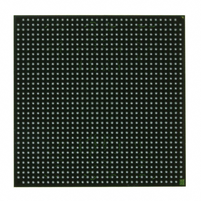
- Package — 1148-BBGA (1148-FCPBGA) flip-chip BGA, 35 × 35 mm, surface-mount package suitable for compact system implementations.
- Power Supply — Core supply range specified at 1.425 V to 1.575 V for predictable power planning and regulator selection.
- Operating Range — Commercial temperature grade: 0 °C to 85 °C for standard commercial deployments.
- Platform Features — Virtex-II Pro family capabilities documented in the datasheet include RocketIO/RocketIO X multi-gigabit transceivers, up to two embedded PowerPC processor blocks, dedicated 18×18 multipliers, digital clock manager (DCM), and SelectRAM™ memory hierarchy.
- Regulatory — RoHS-compliant offering for lead-free assembly requirements.
Typical Applications
- Telecommunications & Datacom — Use the device’s platform transceiver and high I/O count for protocol processing, framing, and multi-channel I/O aggregation.
- Embedded Processing Systems — Leverage the Virtex-II Pro platform’s embedded processor block options and abundant logic to implement control planes and offload tasks from host processors.
- High-Performance Prototyping — Large logic and memory capacity make this FPGA suitable for hardware emulation and design validation of complex digital subsystems.
- Signal Processing and DSP — Dedicated multiplier blocks and plentiful embedded RAM support filtering, transforms, and streaming data paths.
Unique Advantages
- High Logic Density: 43,632 logic elements provide substantial capacity for complex state machines, datapaths, and custom accelerators.
- Extensive I/O: 804 I/O pins enable direct interfacing to multiple peripherals, wide buses, and high-channel-count systems without excessive external serialization.
- On-Chip Memory: Approximately 3.54 Mbits of embedded RAM reduces external memory dependence for many buffering and storage needs.
- Platform-Level Integration: Virtex-II Pro platform features—such as embedded processor blocks and RocketIO transceivers—allow system architects to integrate processing and serial connectivity directly in the FPGA fabric.
- Industry-Standard Package: 1148-ball FCPBGA (35 × 35 mm) supports surface-mount assembly and compact board layout strategies.
- RoHS Compliance: Conforms to lead-free manufacturing requirements for modern electronics production workflows.
Why Choose XC2VP40-5FF1148C?
The XC2VP40-5FF1148C positions itself as a high-capacity Virtex-II Pro FPGA option for commercial designs that need a balance of large logic resources, significant embedded memory, and high I/O density in a standard flip-chip BGA package. Its documented platform features support integration of embedded processing and multi-gigabit serial interfaces, enabling consolidated system architectures.
This device is suited to engineers and procurement teams building communications equipment, embedded compute modules, and high-density prototyping platforms who require precise electrical and thermal planning—core voltage range and operating temperature are explicitly specified to support predictable system design.
Request a quote or submit an inquiry to obtain pricing, availability, and technical support for the XC2VP40-5FF1148C.


Date Founded: 1969
Headquarters: Santa Clara, California, USA
Employees: 25,000+
Revenue: $22.68 Billion
Certifications and Memberships: ISO9001:2015, RoHS, REACH


