
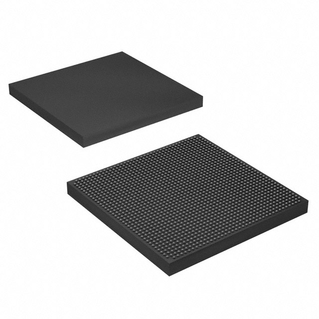
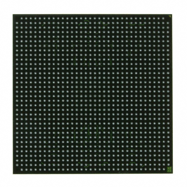
XC4VFX100-10FFG1517C
| Part Description |
Virtex®-4 FX Field Programmable Gate Array (FPGA) IC 768 6930432 94896 1517-BBGA, FCBGA |
|---|---|
| Quantity | 765 Available (as of June 15, 2026) |

| Product Category | Field Programmable Gate Array (FPGA) |
|---|---|
| Manufacturer | AMD |
| Manufacturing Status | Active |
| Manufacturer Standard Lead Time | 14 Weeks |
| Datasheet |
Specifications & Environmental
| Device Package | 1517-FCBGA (40x40) | Grade | Commercial | Operating Temperature | 0°C – 85°C | ||
|---|---|---|---|---|---|---|---|
| Package / Case | 1517-BBGA, FCBGA | Number of I/O | 768 | Voltage | 1.14 V - 1.26 V | ||
| Mounting Method | Surface Mount | RoHS Compliance | ROHS3 Compliant | REACH Compliance | REACH Unaffected | ||
| Moisture Sensitivity Level | 4 (72 Hours) | Number of LABs/CLBs | 10544 | Number of Logic Elements/Cells | 94896 | ||
| Number of Gates | N/A | ECCN | 3A001A7A | HTS Code | 8542.39.0001 | ||
| Qualification | N/A | Total RAM Bits | 6930432 |
Overview of XC4VFX100-10FFG1517C – Virtex®-4 FX FPGA, 1517-FCBGA
The XC4VFX100-10FFG1517C is a Virtex®-4 FX field programmable gate array (FPGA) designed for commercial electronic systems requiring substantial programmable logic, on-chip memory and high I/O count. Its architecture provides a large pool of logic resources and embedded RAM to implement complex digital functions on a single device.
With a 1517-FCBGA surface-mount package and support for a 1.14 V to 1.26 V core supply, this device targets board-level designs where integration density, abundant I/O and significant embedded memory are primary requirements.
Key Features
- Core Logic Provides 10,544 CLBs and 94,896 logic elements for implementing complex digital logic and custom datapaths.
- Embedded Memory Approximately 6.93 Mbits of on-chip RAM to support buffer, FIFO and local storage requirements without external memory.
- I/O Capacity 768 user I/O pins to support wide parallel interfaces, multiple high-pin-count peripherals and dense board connectivity.
- Package & Mounting 1517-FCBGA (1517-BBGA) package in a 40×40 format, intended for surface-mount PCB assembly to minimize board footprint.
- Power Supply Core voltage range of 1.14 V to 1.26 V for compatibility with specified system power rails.
- Operating Range & Compliance Commercial-grade device with an operating temperature range of 0 °C to 85 °C and RoHS compliance for environmental requirements.
Typical Applications
- High-density digital systems Use the device’s 94,896 logic elements to consolidate complex logic and custom processing blocks onto a single FPGA.
- I/O‑intensive interfaces Leverage 768 I/Os for designs requiring many parallel or multiplexed signal connections between system components.
- Memory-demanding functions Apply the approximately 6.93 Mbits of embedded RAM for local buffering, packet storage or intermediate data staging without immediate external memory.
- Compact board-level integration The 1517-FCBGA surface-mount package supports high-density layouts where PCB area and routing density are constrained.
Unique Advantages
- Large programmable resource pool: 10,544 CLBs and 94,896 logic elements allow substantial logic consolidation and complex function implementation.
- Significant on-chip RAM: Approximately 6.93 Mbits of embedded memory reduces dependence on external memory for many designs.
- Extensive I/O availability: 768 I/Os enable broad interfacing options and support for multiple parallel channels.
- Compact FCBGA package: The 1517-FCBGA (40×40) surface-mount package supports dense board integration and optimized PCB real estate usage.
- Commercial temperature and RoHS compliance: Rated for 0 °C to 85 °C operation and RoHS compliant to meet common commercial product requirements.
Why Choose XC4VFX100-10FFG1517C?
The XC4VFX100-10FFG1517C positions itself as a high-density, commercially graded FPGA option for designers who need large logic capacity, ample embedded memory and substantial I/O in a compact surface-mount package. Its specification set is well suited to board-level systems where consolidating functions into a single programmable device reduces BOM complexity and preserves PCB area.
This device is a suitable choice for engineering teams building scalable digital designs that require on-chip RAM, broad I/O connectivity and a verified commercial operating range, offering predictable integration into established development flows.
Request a quote or submit an inquiry to receive pricing and availability information for XC4VFX100-10FFG1517C and support for your design requirements.


Date Founded: 1969
Headquarters: Santa Clara, California, USA
Employees: 25,000+
Revenue: $22.68 Billion
Certifications and Memberships: ISO9001:2015, RoHS, REACH


