
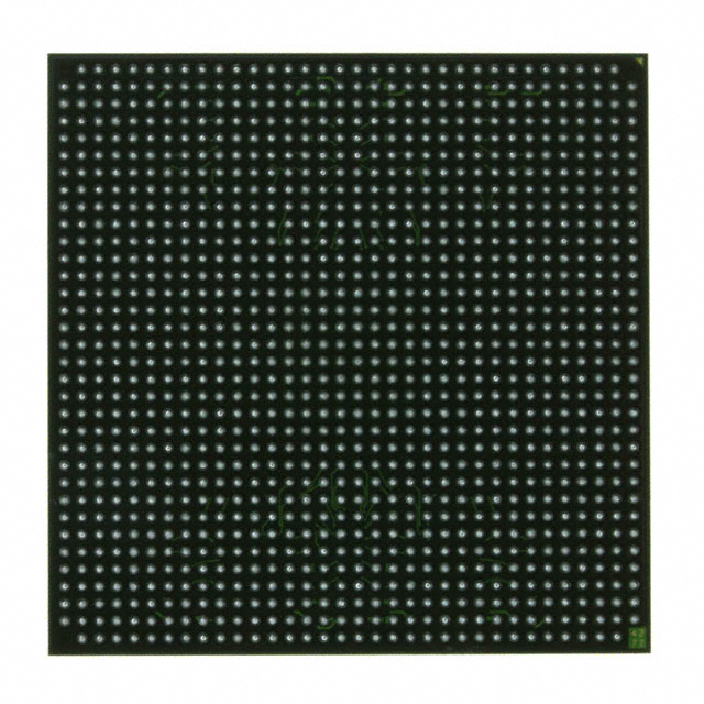
XC4VFX60-10FF672C
| Part Description |
Virtex®-4 FX Field Programmable Gate Array (FPGA) IC 352 4276224 56880 672-BBGA, FCBGA |
|---|---|
| Quantity | 930 Available (as of June 14, 2026) |

| Product Category | Field Programmable Gate Array (FPGA) |
|---|---|
| Manufacturer | AMD |
| Manufacturing Status | Active |
| Manufacturer Standard Lead Time | 12 Weeks |
| Datasheet |
Specifications & Environmental
| Device Package | 672-FCBGA (27x27) | Grade | Commercial | Operating Temperature | 0°C – 85°C | ||
|---|---|---|---|---|---|---|---|
| Package / Case | 672-BBGA, FCBGA | Number of I/O | 352 | Voltage | 1.14 V - 1.26 V | ||
| Mounting Method | Surface Mount | RoHS Compliance | RoHS non-compliant | REACH Compliance | REACH Unaffected | ||
| Moisture Sensitivity Level | 4 (72 Hours) | Number of LABs/CLBs | 6320 | Number of Logic Elements/Cells | 56880 | ||
| Number of Gates | N/A | ECCN | 3A991D | HTS Code | 8542.39.0001 | ||
| Qualification | N/A | Total RAM Bits | 4276224 |
Overview of XC4VFX60-10FF672C – Virtex®-4 FX Field Programmable Gate Array, 672-FCBGA (27×27)
The XC4VFX60-10FF672C is a Virtex®-4 FX field programmable gate array (FPGA) in a 672-ball FCBGA package designed for commercial-grade embedded logic applications. It integrates 56,880 logic elements and approximately 4.28 Mbits of on-chip RAM, alongside 352 user I/O pins, enabling complex custom logic, buffering and interfacing in a single device.
With a 1.14 V to 1.26 V core voltage range, surface-mount 672-FCBGA (27×27) package, and a 0 °C to 85 °C operating range, this FPGA is targeted at designs that require high-density programmability with defined commercial-temperature operation and RoHS compliance.
Key Features
- Core Logic 56,880 logic elements provide programmable resources for implementing custom digital functions, state machines, and data-paths.
- Embedded Memory Approximately 4.28 Mbits of on-chip RAM for FIFOs, buffers, and local data storage to support high-throughput logic designs.
- I/O Density 352 user I/O pins for broad system interfacing, enabling multiple parallel data channels and flexible signal routing.
- Power Supply Core voltage supply range of 1.14 V to 1.26 V to match platform power budgeting and regulator designs.
- Package & Mounting 672-ball FCBGA (27×27) surface-mount package for compact board-level integration and high pin-count density.
- Operating Range & Grade Commercial-grade device rated for 0 °C to 85 °C operation, suitable for a wide range of commercial embedded systems.
- Environmental Compliance RoHS compliant, supporting lead-free assembly and regulatory requirements for many commercial products.
Typical Applications
- Data and signal processing systems Use the 56,880 logic elements and on-chip RAM to implement custom data-paths, packet processing, and buffering functions.
- Embedded control and interfacing Leverage 352 I/O pins for connecting sensors, peripherals, and external devices while consolidating glue logic into the FPGA fabric.
- Custom protocol bridging Deploy programmable logic to implement protocol translators, timing adaptation, and bespoke serial/parallel interfaces within a single device.
- Prototyping and system integration High logic density and embedded memory make the device useful for developing and validating complex hardware algorithms and system prototypes.
Unique Advantages
- High-density programmable logic: 56,880 logic elements enable integration of sizable custom functions and hardware accelerators without multiple discrete components.
- On-chip memory resources: Approximately 4.28 Mbits of embedded RAM reduce external memory dependency for buffering and temporary storage, simplifying board design.
- Extensive I/O count: 352 user I/O pins provide flexibility for multi-channel interfaces and parallel data paths, minimizing external interface components.
- Compact package: 672-FCBGA (27×27) offers a high pin-count solution in a compact footprint for space-constrained PCB layouts.
- Commercial suitability: Rated for 0 °C to 85 °C operation and RoHS compliant for deployment in commercial embedded products.
Why Choose XC4VFX60-10FF672C?
The XC4VFX60-10FF672C positions itself as a high-density, commercially-graded Virtex-4 FX FPGA option providing a balanced combination of programmable logic, embedded memory, and I/O resources in a 672-ball FCBGA package. Its specification set—56,880 logic elements, approximately 4.28 Mbits of on-chip RAM, 352 I/Os, and a defined core voltage range—makes it suitable for engineers building complex digital systems that require substantial on-chip resources and flexible interfacing.
For designers focused on integrating substantial custom logic and buffering within a single, RoHS-compliant device footprint, this FPGA offers a clear hardware platform to consolidate functions, reduce component count, and accelerate system-level development.
Request a quote or submit an inquiry to receive pricing and availability information for the XC4VFX60-10FF672C and to discuss how it can meet your design requirements.


Date Founded: 1969
Headquarters: Santa Clara, California, USA
Employees: 25,000+
Revenue: $22.68 Billion
Certifications and Memberships: ISO9001:2015, RoHS, REACH


